Alphabetical Index
Browse by Elements
Keyword Search
Dry Etchants
Dry and Wet Etchants
Wet Etchants
Bulk Etchants
Layer Etchants
Nano Etchants
Single Crystal Etchants
Thin Film Etchants
Thin Foil Etchants
Wafer Etchants
Al Etchants
Cd Etchants
Ga Etchants
Ge Etchants
In Etchants
New Etchants
Other Etchants
Si Etchants
Zn Etchants
Help
Home
InP Layer - Dry Etching - Demo Record
Material Name: InP
Recipe No.: 9890
Primary Chemical Element in Material: InP
Sample Type: Layer
Uses: Etching
Etchant Name: None
Etching Method: Dry etching
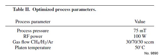
Etchant (Electrolyte) Composition: See the Table 1.
Procedure (Condition): No data
Note: In this paper we present a novel single-step RIE process for InP membrane optical waveguide etching. The optimization of the
process is focused on the sidewall verticality and surface roughness of the etched profile. Significant improvement on the etched
profile is achieved for the first time in a single-step RIE process. Loss measurement on fabricated membrane waveguides etched with
the proposed RIE process results in a record low waveguide propagation loss (2.5 dB/cm).
Reference: Yuqing Jiao, et al., Vertical and Smooth Single-Step Reactive Ion Etching Process
for InP Membrane Waveguides, Journal of The Electrochemical Society, 162 (8) E90-E95 (2015).
Other our software: Metal Etchants v.5.0
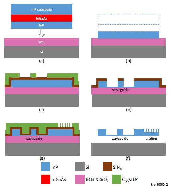
Figure 1: The fabrication process for InPmembrane
waveguides. (a) wafer bonding (b) InP substrate and
InGaAs sacrificial layer removal (c) 1st EBL for
waveguides (d) Waveguide etching (e) 2nd EBL for
gratings (f) Final device after grating etching.
Table 1: Optimized process parameters.