Alphabetical Index
Browse by Elements
Keyword Search
Dry Etchants
Dry and Wet Etchants
Wet Etchants
Bulk Etchants
Layer Etchants
Nano Etchants
Single Crystal Etchants
Thin Film Etchants
Thin Foil Etchants
Wafer Etchants
Al Etchants
Cd Etchants
Ga Etchants
Ge Etchants
In Etchants
New Etchants
Other Etchants
Si Etchants
Zn Etchants
Help
Home
Al2O3/TiO2 - Dry and Wet Etching
Material Name: Al2O3/TiO2
Recipe No.: 10297
Primary Chemical Element in Material: Al, Ti
Sample Type: Layer
Uses: Etching
Etchant Name: None
Etching Method: Dry and wet etching
Etchant (Electrolyte) Composition: To evaluate the level of surface passivation, 100 Wcm n-type float zone <100> crystalline Si (c-Si)
wafers were used to measure the emitter saturation current density. A p+np+ structure with a sheet
resistance of 230 W/sq was obtained after a boron di.usion and drive in processes, and was coated
with Al2O3/TiO2 stack layers on both sides. Prior to deposition, the Si substrates were cleaned with a
standard RCA (Radio Corporation of America) process followed by rinsing in deionized water and a
dipping in a dilute HF solution at room temperature. The Al2O3/TiO2 stack films were deposited by
thermal ALD, and the substrate temperature was maintained over the temperature range of 100–300 C
using H2O as the oxidant source. The feeding and purge times were controlled to achieve a self-limiting
ALD process at each deposition temperature. To measure the wet etch rate, the film thicknesses were
measured by spectroscopic ellipsometry using a HORIBA Scientific UVISEL system. The measurements
were taken with an incident angle of 70. over an illumination wavelength range of 200–1000 nm.
From the ellipsometric data to a model given by HORIBA Scientific, both film thicknesses which are the
real part of the refractive index were determined, while the imaginary part of the refractive index was
fixed to the parameters of the model. Unless otherwise stated, all Al2O3 and TiO2 films had a thickness
of 10 nm and 50 nm, respectively. Because the growth rate of thermal ALD is generally dependent on
the deposition temperature, the number of cycles was optimized to reach a self-limiting ALD process
and target thickness at di.erent deposition temperatures. Surface passivation was evaluated in
the as-deposited state and after 30 min post-deposition annealing at 300–730 C in an O2 environment.
The plasma etching experiments were performed in a chamber utilizing an inductively-coupled
plasma source operating at 2 MHz and 500 W as well as a radio frequency of 13.56 MHz of at a power
of 100 W. Each sample was etched using 50 sccm CHF3 and 10 sccm Ar at a low pressure of 5 mTorr.
The SC2 cleaning methodology developed at RCA laboratories is a procedure for removing metal
impurities from a silicon surface. The cleaning process is based on the sequential oxidative desorption
and complexing with H2O2:HCl:H2O (volumetric ratio 1:1:5). This process is generally preceded
by an SC1 clean using a H2O2:NH4OH:H2O (volumetric ratio 1:1:5) solution to remove any organic
residues. In the meantime, the chemical oxide is removed without damaging the surface using a HF
etchant followed by rinsing in de-ionized water. RCA and HF etching were used to examine the etching
characteristics of TiO2 on amorphous Al2O3. The blistering phenomenon as well as the morphology of
the thin film surface before and after etching were examined by optical microscopy (Olympus BX 40),
scanning electron microscope (SEM), and atomic force microscopy (AFM). The passivation properties
of the stacks after etching were evaluated by measuring the photoluminescence by LIS-R (BT imaging)
and the implied open circuit voltage using the photoconductance decay method.
Dry Etching
Figure 1 presents the TiO2 dry etch rates on amorphous Al2O3 under different deposition and
annealing conditions. The etch rates of samples deposited at 200–300 C were almost independent
of the post-deposition annealing step regardless of the annealing temperature. This indicates that
polycrystalline TiO2 deposited over 200 C is more resistant to reactive species during dry etching than
amorphous TiO2 deposited at 100 C. As a result, the deposition temperature is more important
for determining the etch resistance than post-heat treatment. In the case of TiO2 samples deposited at
100 C, the minimum etch rate was obtained from 400 C annealing.
Figure 2 presents the dry etch rates of TiO2 and Al2O3 films as a function of the etch time and
deposition temperature. TiO2 and Al2O3 single layers with a thickness of 200 nm were deposited at
200 C without a post-deposition annealing step, and Figure 2 shows TiO2 layers on Al2O3 deposited
at a deposition temperature of 100–300 C. The selectivity for etching TiO2 over Al2O3 in CHF3 and Ar
gas was not remarkable, compared to chemical etching. The dry etch rates of the TiO2 films on Al2O3
were approximately double those of Al2O3 in all samples deposited at different temperature ranges.
The etch rates tended to decrease slightly with increasing TiO2 deposition temperature. In the case of a
200-nm-thick TiO2 single layer, the etch rates were 1.1–1.2 nm/s, which were higher than those of the
50 nm-thick TiO2 films on Al2O3. This is because the film density increases with an increasing number
of deposition cycles during the ALD process, i.e., with increasing film thickness. Therefore, thicker TiO2 films are more resistant than thinner films. The etch rate of the Al2O3 single layer was almost
independent of the etch time.
Wet Etching
Wet chemical etching process is currently the standard procedure for mass production lines of
crystalline silicon solar cells. For example, an alkaline or acidic etching mixture is commonly used for
surface texturing; a low concentrated HF solution is used for phosphorus silicon glass removal; an
acidic mixture is utilized for edge isolation by single-side etching. The pre-cleaning of crystalline
silicon wafers is also essential for the elimination of residue and subsequent process homogeneity.
Most alkaline cleaning solutions are similar to SC1 in semiconductor processes, and HF dipping is used
to clean hydrophilic wafer surfaces. Several cleaning steps have been introduced to further optimize
the e.ciency potential of PERC-based screen-printed silicon solar cells. Nevertheless, it is important
investigate the etching characteristics because a range of chemical solutions have been developed
for these cleaning processes.
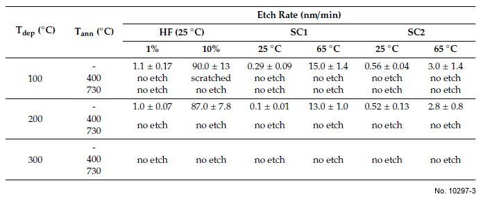
Table 1 lists the variation of the etch rates of the TiO2 layer on amorphous Al2O3 in HF, SC1, and
SC2 with di.erent concentrations and temperatures. Most films deposited at 300 C generally showed
extremely low etch rates exhibiting overall resistance to chemical etching. The maximum etch rate
of TiO2 deposited at 100 C was 90 nm/min using a 10% HF solution at room temperature. The TiO2
etch rate decreased with decreasing HF concentration, and increased with decreasing deposition and
annealing temperature as well as etching temperature. The etch rate in SC1 was half and five times at
an etching temperature of 25 C and 65 C, respectively, than that in SC2.
Procedure (Condition): No data
Note: Chemical processes are very important for the development of high-e.ciency crystalline
solar cells, mainly for surface texturing to improve light absorption and cleaning processes to reduce
surface recombination. Recently, research has been focusing on the impact of chemical polishing
on the performance of a passivated emitter and rear cells (PERC), with particular emphasis on the
dielectric passivation layers on the front side. This study examined the influence of etching on the
passivation of Al2O3/TiO2 stacks, where the films may each be deposited using a range of deposition
and post-annealing parameters. Most TiO2 films deposited at 300 .C were resistant to chemical
etching, and higher temperature deposition and annealing produced more chemical-resistant films.
TiO2 films deposited at 100 C were etched slightly by SC1 and SC2 solutions at room temperature,
whereas they were etched at a relatively high rate in an HF solution, even when capped with a thick
TiO2 layer (up to 50 nm in thickness); blistering occurred in 20-nm-thick Al2O3 films. In contrast to
the as-deposited films, the annealed films showed a lower level of passivation as 1% HF etching
proceeded. The implied open circuit voltage of the samples annealed at 300 C after HF etching
decreased more than those annealed at 400 C. The dark area in the photoluminescence images was
not resistant to the HF solution and showed more etch pits. The etching strategies developed in this
study are expected to help setup integration processes and increase the applicability of this stack to
solar cells.
Reference: Dongchul Suh, Etch Characteristics and Morphology of Al2O3/TiO2
Stacks for Silicon Surface Passivation, Sustainability 2019, 11, 3857; doi:10.3390/su11143857.
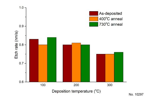
Figure 1: TiO2 dry etch rates on amorphous Al2O3 as a function of the deposition temperature under
di.erent annealing conditions.
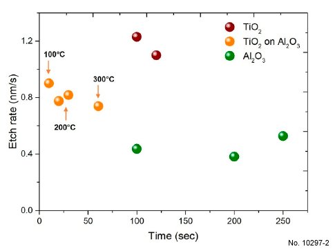
Figure 1: Dry etch rates of TiO2 (in types of single layer and stack) and Al2O3 single layer as a function
of the etching time. The TiO2 deposition temperatures of stack samples are also presented.
Table 1: Wet etch rate to several chemical solutions as a function of the deposition temperature under
di.erent annealing conditions.