Alphabetical Index
Browse by Elements
Keyword Search
Dry Etchants
Dry and Wet Etchants
Wet Etchants
Bulk Etchants
Layer Etchants
Nano Etchants
Single Crystal Etchants
Thin Film Etchants
Thin Foil Etchants
Wafer Etchants
Al Etchants
Cd Etchants
Ga Etchants
Ge Etchants
In Etchants
New Etchants
Other Etchants
Si Etchants
Zn Etchants
Help
Home
Cr Layer - Dry Etching
Material Name: Cr
Recipe No.: 10298
Primary Chemical Element in Material: Layer
Sample Type: Layer
Uses: Etching
Etchant Name: None
Etching Method: Dry etching
Etchant (Electrolyte) Composition: The etching of thick Cr layers at a submicron scale has not been performed in detail so far,
partly due to the hardness of Cr, which makes the etching difficult. Furthermore, the following
deep oxide etching process necessitates a large Cr thickness (>= 150 nm), which leads to aspect
ratios of 0.5 for the 300 nm-large pores and 1 for the 150 nm-thick pore walls. Such aspect
ratios are very high for a metal layer. Taking into account the small resist thickness limited by
the e-beam lithography process, and the diversity of the resists used in this project, we had to
find an optimal procedure, allowing to etch small features in Cr with aspect ratios around 0.5
and a selectivity better than 1:3 to any kind of resist. Furthermore, the etching of small samples
requires the samples to be glued on a 4” substrate, e.g., a silicon dummy wafer. Since the glue
used possess a low thermal conduction, the process to be designed should also be temperature
independent.
Procedure (Condition): No data
Note: No data
Reference: Electron-Beam Lithography, Experimental Fabrication, pp. 69-89, Source not known.
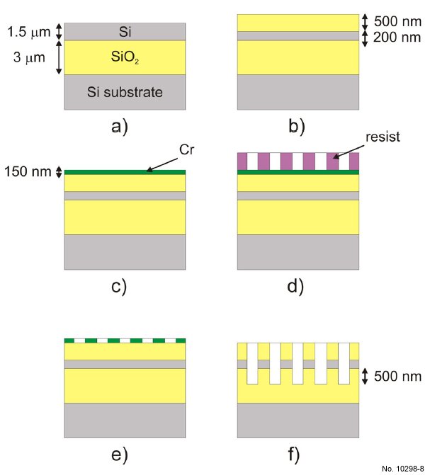
Figure 1: Full process designed to fabricate the IOSOI PPCs. a) Initial SOI wafer, b) formation of the
silicon core and the upper oxide cladding via thermal oxidation steps followed by wet etching in HF, c)
deposition of the Cr mask by sputtering, d) electron-beam lithography, e) patterning of the Cr mask and
f) patterning of the IOSOI structure.
Table 1: Starting recipe used for the optimization of the Cr etching process.
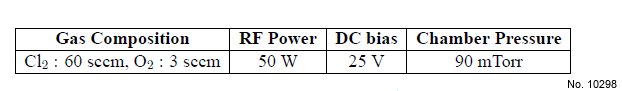
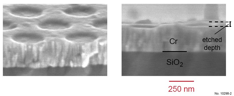
Figure 2: Cross sectional SEM images of the sample after Cr etching with the recipe optimized for
larger feature sizes (given in table 1). The left picture was obtained by tilting the sample 15 deg. towards
the surface.
Table 2: Results of the Cr etching using the optimized recipe and the three types of resists.
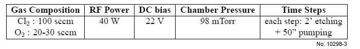
Table 3: Optimized recipe used for the Cr etching process.
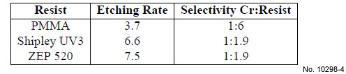
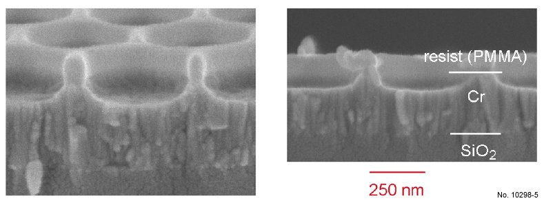
Figure 3: Cross sectional SEM images of the sample after Cr etching using the optimized recipe and
a 700 nm-thick PMMA mask. The total thickness of the Cr layer was 400 nm. The left picture was
obtained by tilting the sample 15. towards the surface.
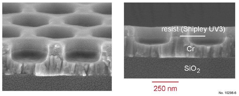
Figure 4: Cross sectional SEM images of the sample after Cr etching using the optimized recipe and
a 350 nm-thick Shipley UV3 mask. The total thickness of the Cr layer was 400 nm. The left picture was
obtained by tilting the sample 15. towards the surface.
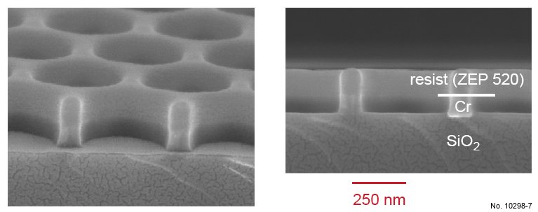
Figure 5: Cross sectional SEM images of the sample after Cr etching using the optimized recipe and
a 400 nm-thick ZEP 520 mask. The total thickness of the Cr layer was 140 nm. In this case, the resist
layer was thick enough to etch through the whole Cr layer. The left picture by obtained via tilting the
sample 15. towards the surface.