Alphabetical Index
Browse by Elements
Keyword Search
Dry Etchants
Dry and Wet Etchants
Wet Etchants
Bulk Etchants
Layer Etchants
Nano Etchants
Single Crystal Etchants
Thin Film Etchants
Thin Foil Etchants
Wafer Etchants
Al Etchants
Cd Etchants
Ga Etchants
Ge Etchants
In Etchants
New Etchants
Other Etchants
Si Etchants
Zn Etchants
Help
Home
Silicon and Silicon Dioxide Etching - Dry Etching
Material Name: Si, SiO2
Recipe No.: 10299
Primary Chemical Element in Material: Si
Sample Type: Wafer, layer
Uses: Etching
Etchant Name: None
Etching Method: Dry etching
Etchant (Electrolyte) Composition: Similar to Cr etching, silicon-dioxide etching at a submicron scale with high aspect ratios is a
challenging process, although the etching of thin SiO2 layers with low aspect ratios is a standard
process of the silicon technology. This is due to two main issues that become stronger
with increasing aspect ratio. First, since SiO2 is an insulator, the pore walls bombarded by the
incident particles become charged during the process. Secondly, the etch products react
with the plasma particles to form a polymer that redeposits on the pore walls. Both issues
are well-known and have been widely studied. However, no satisfying general solution has been
proposed so far. Since the fabrication of the IOSOI-based PPCs requires deep oxide etching,
we should design an etching process which overcomes these two problems. Furthermore, the
etching process should allow smooth transitions between the three layers SiO2/Si/SiO2, without
underetching at the interfaces, to achieve perfectly vertical walls in the thin silicon core.
The etching is performed in an Oxford Plasmalab System 100 machine with the ICP380 source,
equipped with fluorine-based gases. Unlike the case of Cr etching, no systematic study has been
performed for the SiO2/Si/SiO2 etching. This is due to the wide choice in chemistry involved
in the etching process, leading to a large number of parameters that have to be optimized.
Furthermore, several issues have to be addressed simultaneously, such as the etching of two
different materials with completely different properties, Si and SiO2, and the transitions between
these two materials. Therefore, the method used was first to vary the parameters arbitrarily, to
understand their influence on the etching results and to determine basic recipes. Among the
several processes tested, one RIE process and two basic ICP processes were selected. These
processes were then optimized further. This study is presented in more details in the following sections.
Results for RIE Etching: Initially, we intended to etch the three-layer structure SiO2/Si/SiO2 in one step. Therefore, all
the recipes under study - RIE as well as ICP - should allow to etch SiO2 as well as Si. In order to test both the deep oxide etching and the transition SiO2/Si with limited costs, all the etching tests were first performed on oxidized dummy silicon wafers with 1.5 µm SiO2 on the top. The SOI
wafers were used after optimization of the process. The parameters of the optimized recipe for
RIE etching are summarized in table 4.5, and SEM pictures of the etched samples are presented
in fig. 4.16. This process shows the advantage to well preserve the Cr mask. Furthermore,
the pore profiles presented in fig. 4.16 are vertical and only small polymer redeposition can be
observed. However, if the pore depth is deeper than 500-600 nm, the profile becomes very bad
and the pores tend to close, as shown in fig. 4.17. This ”carrot” profile is found in most RIE
processes that have been studied in this work and is also observed very often when etching III-V
compounds in the RIE mode. Therefore, the RIE process is restricted to low aspect ratios up to 1.5.
Results for ICP Etching: In parallel to the RIE mode, the ICP etching was studied. Two basic recipes were selected,
based on the CHF3/SF6 and C4F8/Ar chemistry, respectively. For a better understanding of the
different mechanisms that occur during etching, we will discuss the optimization of the first
type of recipe in more details. The basic parameters for this recipe are summarized in table 4.6.
SEM pictures of the samples after etching are presented in fig. 4.18.
Using the recipe presented in table 4.6, 900 nm oxide layers were etched, corresponding to an
etching rate of 75 nm/min. As can be noticed in fig. 4.18, this recipe is not very aggressive against the Cr mask, since only 20-30 nm have been removed. However, the ”bottle-shape” of
the oxide walls is typical for a charging of the walls during the etch process. Since SiO2 is
an insulator, it can be strongly charged by the plasma particles reaching the pore walls. As a
consequence of the wall charging, the plasma particles are deflected, leading to this particular
profile. One of the ways to avoid this problem is to increase the energy of the particles to
enhance the anisotropy and reduce the amount of particles reaching the pore walls instead of
the pore bottom. This is achieved by enhancing the bias, i.e., by enhancing the RF power, or
by decreasing the pressure. Furthermore, the roughness on the top part of the walls, that can be
observed in fig. 4.18, is due to some polymer formation and redeposition. This phenomenon
is typical for SiO2 etching with carbon-based gases. A way to lower this effect is to reduce
the carbon concentration in the plasma. Therefore, in the following recipe, the SF6 flow was
enhanced. The parameters of this recipe with increased RF power and increased SF6 flow are
presented in table 4.7, and SEM pictures of the sample after etching are shown in fig. 4.19.
As can be noticed in fig. 4.19, the etching rate is strongly enhanced due to the higher bias,
and the underlying silicon layer was reached. It can be clearly recognized that this recipe
allows to etch SiO2 as well as Si. However, the Cr mask was almost completely sputtered away
during the etching process. As a result, the upper part of the oxide walls was partly removed,
and the remaining walls are not perfectly vertical. Therefore, a very high bias is not a good
solution to avoid the ”bottle” profile of the walls arising from the particle deflection. In a
further optimization of the ICP process, the parameters should be chosen in such a way that
the Cr mask holds during the etching process. A possible solution is to vary the bias during
the process. In this way, the trajectory of the charged particles can be modified continuously to
avoid a ”bottle” profile, with an average bias low enough to protect the Cr mask. The parameters
of the recipe with varying RF power are presented in table 4.8, and SEM pictures of the sample after etching are shown in fig. 4.20.
Comparing with fig. 4.18, the profile of the oxide walls in fig. 4.20 is much better. However, as
could also be observed in fig. 4.19, the two last recipes lead to a strong polymer redeposition on
the upper part of the oxide walls. Furthermore, large underetching of the silicon at the interface
SiO2/Si occurred with the recipe presented in table 4.8. Due to the strong bias of the recipe
given in table 4.7, the transition between the SiO2 and the Si layers was much smoother. A way
to reduce the underetching observed in fig. 4.20, without increasing the bias, is to add some
oxygen in the plasma. Indeed, oxygen is often used in deep silicon etching, to passivate the
silicon walls during the etching process and to protect them. Since O2 plasmas are also used to
etch polymers, we hope that adding O2 in the plasma will simultaneously reduce the polymer
redeposition. The parameters of the new recipe, with additional O2 in the plasma and an average
RF power of 65 W, are presented in table 4.9. The corresponding SEM pictures of the sample
after etching are shown in fig. 4.21.
Although the underetching is reduced with additional O2 in the plasma, the polymer redeposition
is still as strong as was observed in fig. 4.19 and fig. 4.20. Replacing CHF3 by C4F8 in
the above processes, very smooth transitions without any underetching at the SiO2/Si interfaces
were achieved. However, the polymer redeposition was not reduced. Another solution to this
problem is to reduce again the carbon concentration in the plasma. The corresponding recipe is
given in table 4.10. From the results presented in fig. 4.22, it can be deduced that this solution
strongly limits the polymer formation. However, the shape of the pores is tilted. This is partly
due to the removing of the Cr mask, partly to the modification of the process chemistry.
To summarize, the optimized recipe based on the CHF3/SF6 chemistry should yield simultaneously:
• Perfectly vertical walls. It implies a preserved Cr mask, as well as no ”bottle” profile.
This is achieved by working with an average low bias, and by varying it (i.e., varying
the RF power) during the process to modify continuously the trajectory of the deflected
particles.
• No underetching of the silicon at the interface SiO2/Si. A way to reduce this underetching
is to apply very high bias when etching through the interface between the two materials.
The other way is to modify the gas composition, by replacing CHF3 by C4F8. The addition
of O2 in the plasma, to passivate the silicon walls during the etching process, can also
help.
• A limited polymer formation and redeposition on the pore walls. This issue is the most
difficult one. Although the presence of the polymer on the upper part of the oxide walls
may not have any significant influence on the device functionality, it may strongly affect
the properties of the PPC if it is deposited in the surrounding of the Si core. A possible
solution to limit the polymer formation is to lower the carbon concentration in the
plasma. However, a good compromise between low redeposition requiring low carbon
concentration, and vertical walls requiring high carbon concentration, still remains to be
found.
Although the further optimization of this ICP process may be possible in order to find a recipe
fulfilling all requirements cited above, we prefer to study a second type of process based on the C4F8/Ar chemistry. The basic recipe for this second ICP process is given in table 4.11.
In the case of C4F8 highly diluted in a noble gas like Ar, the plasma chemistry is completely
different from the previous case. In particular, the polymer redeposition is very homogeneous
and passivates the pore walls in a convenient way, leading to a high anisotropy and a good
protection of the walls from underetching at the interfaces. As a result, the pore walls are
smooth and highly vertical, and the transitions at the interfaces between the silicon and the
oxide are not visible. Furthermore, during this process the Cr mask is well preserved, allowing
deep anisotropic etching. The same recipe applied to SOI wafers led to similar results, as
confirmed in fig. 4.23.
Procedure (Condition): No data
Note: No data
Reference: Electron-Beam Lithography, Experimental Fabrication, pp. 69-89, Source not known.
Table 4.5: Recipe of the optimized RIE process for SiO2/Si etching.
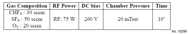
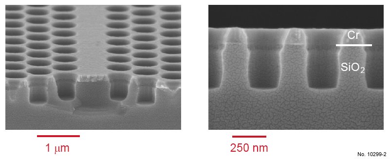
Figure 4.16: Cross sectional SEM images of SiO2 etching with the RIE recipe presented in table 4.5.
The left picture was obtained by tilting the sample 15 deg. towards the surface, and a W1 waveguide can be
recognized in its center.
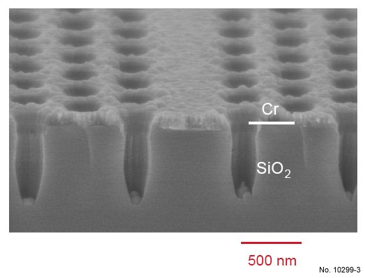
Figure 4.17: Cross sectional SEM image of SiO2 etching with the RIE recipe presented in table 4.5 and
a longer etching time. The picture was obtained by tilting the sample 15 deg. towards the surface, and a W1
waveguide can be recognized in its center.
Table 4.6: First ICP etching basic recipe used for SiO2/Si etching.
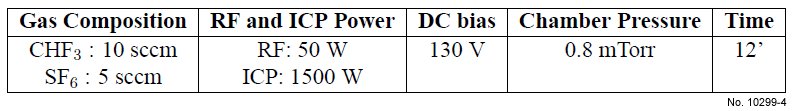
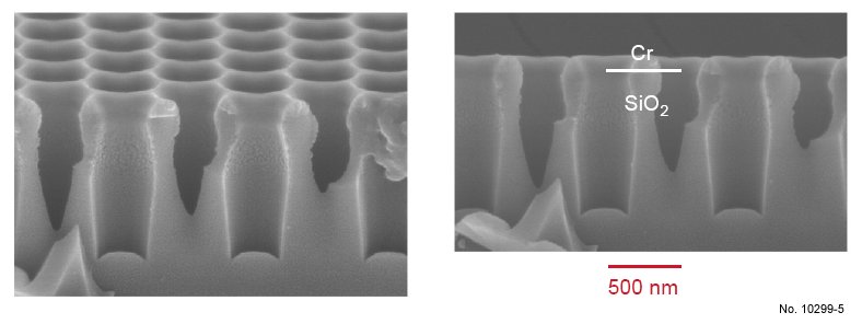
Figure 4.18: Cross sectional SEM images of SiO2 etching with the ICP recipe presented in table 4.6.
The left picture was obtained by tilting the sample 15 deg. towards the surface.
Table 4.7: Second ICP etching basic recipe used for SiO2/Si etching, with increased RF power and SF6
concentration.
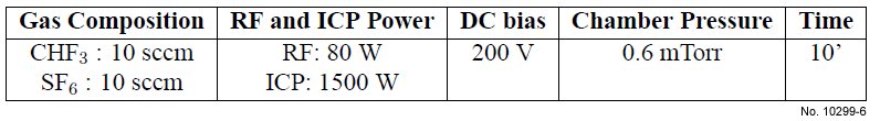
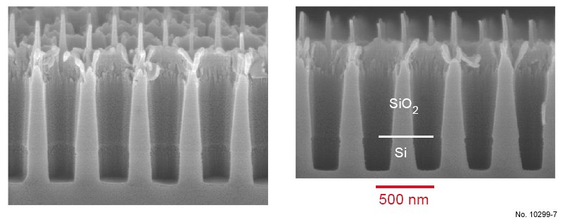
Figure 4.19: Cross sectional SEM images of SiO2/Si etching with the ICP recipe presented in table 4.7.
The left picture was obtained by tilting the sample 15 deg. towards the surface.
Table 4.8: ICP etching recipe used for SiO2/Si etching, with varying RF power.
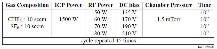
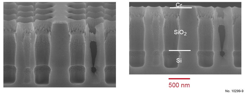
Figure 4.20: Cross sectional SEM images of SiO2/Si etching with the ICP recipe presented in table 4.8.
The left picture was obtained by tilting the sample 15 deg. towards the surface. In the center of the pictures,
a W1 waveguide can be recognized.
Table 4.9: Recipe of the ICP etching process for SiO2/Si etching, with O2 in the gas mixture.
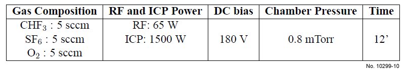
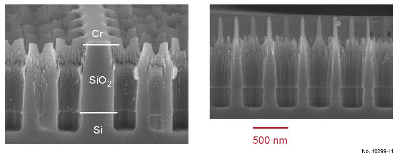
Figure 4.21: Cross sectional SEM images of SiO2/Si etching with the ICP recipe presented in table 4.9.
The left picture was obtained by tilting the sample 15 deg. towards the surface, and a W1 waveguide can be
recognized in its center.
Table 4.10: ICP etching recipe used for SiO2/Si etching, with varying RF power and a lower CHF3
concentration.
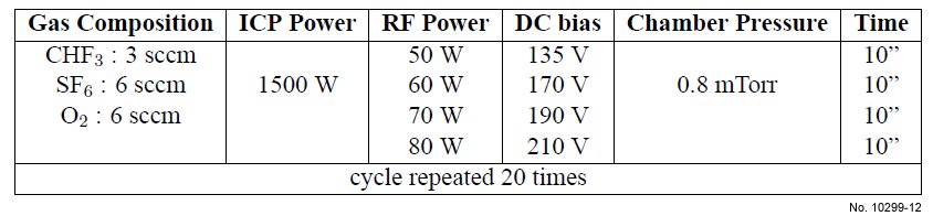
Figure 4.22: Cross sectional SEM image of SiO2/Si etching with the ICP recipe presented in table 4.10.
The picture was obtained by tilting the sample 15 deg. towards the surface, and a W1 waveguide can be
recognized in its center.
Table 4.11: Second type of ICP etching recipe used for SiO2/Si etching, based on the C4F8/Ar chemistry.
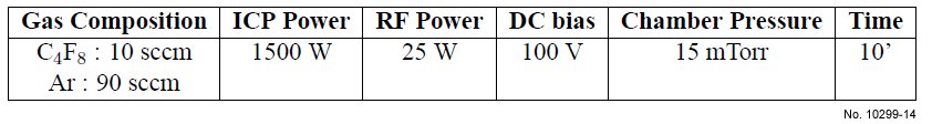
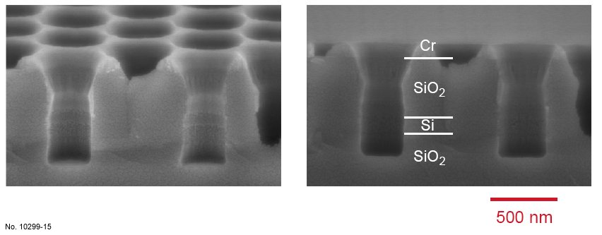
Figure 4.23: Cross sectional SEM images of SiO2/Si/SiO2 etching with the ICP recipe presented in table
4.11. The left picture was obtained by tilting the sample 15 deg. towards the surface.