Alphabetical Index
Browse by Elements
Keyword Search
Dry Etchants
Dry and Wet Etchants
Wet Etchants
Bulk Etchants
Layer Etchants
Nano Etchants
Single Crystal Etchants
Thin Film Etchants
Thin Foil Etchants
Wafer Etchants
Al Etchants
Cd Etchants
Ga Etchants
Ge Etchants
In Etchants
New Etchants
Other Etchants
Si Etchants
Zn Etchants
Help
Home
Diamond Thin Film - Laser Etching
Material Name: Diamond
Recipe No.: 10305
Primary Chemical Element in Material: C
Sample Type: Thin film
Uses: Etching
Etchant Name: None
Etching Method: Laser etching
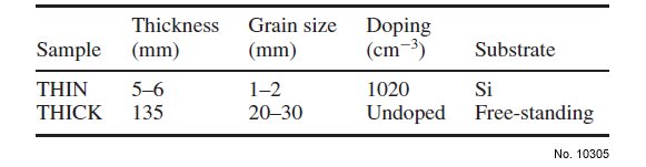
Etchant (Electrolyte) Composition: Two thicknesses of thin film diamond deposited by the
technique of microwave plasma enhanced chemical vapour
deposition (MWPECVD) have been employed in this
study. The properties of these two films designated THIN
and THICK are summarized in table 1. Both types of
films displayed a morphology consisting of randomly aligned
coalesced crystallites. Prior to laser processing and subsequent
characterization, the samples were subjected to a wet etching
treatment consisting of immersion in a saturated solution
of H2SO4:NH4(SO4) (30 min, 200 C) followed by a
H2O2:NH4OH solution (15 min, boiling); this has been shown
to remove surface graphitic layers. An excimer laser
(Lambda Physik LPX305i) operating at 193 nm (ArF) with
an average pulse duration of 20 ns was used throughout. The
output beam of the laser system, measuring 20 mm ~ 10 mm,
was directed onto a chrome-on-quartz mask; the mask pattern
was then directly projected via a 10:1 reduction lens system
(NA = 0.05) onto the sample placed on a microprocessor
controlled x-y-z stage. The system has been described in
more detail elsewhere. SEM images were recorded using
a Hitachi S800 instrument; film profiling was carried out
using a Tencor Instrument profilometer. Raman scattering
analysis was performed with a Renishaw System 2000 Raman
spectrometer (He.Ne (632.8 nm) laser excitation). AES was
carried out in an ultra-high vacuum (UHV) chamber with a
base pressure 5 x 10 exp(-10) Torr. A primary electron beam
energy of 3 kV was used throughout with a low beam current
(1 µA) to minimize electron induced damage within the
surface region; a Varian 981-2707 cylindrical mirror analyser
(CMA) and associated electronics was used to produce
differential Auger spectra. Electrical measurements were
made using a Hewlett Packard HP4140B semiconductor
parameter analyser.
Procedure (Condition): No data
Note: Excimer laser projection patterning with an ArF (193 nm) source has been
employed in the irradiation of thin diamond films. The effect of a number of
process parameters including laser fluence and processing ambient on the
quality of the etch product has been investigated; scanning electron
microscopy shows that good control of etch quality may be achieved with
excellent lateral reproduction of images down to 2 ìm. Raman scattering
and Auger electron spectroscopy of irradiated films have been correlated,
and modifications in the diamond surface have been quantified according to
processing parameters. Electrical tests on laser modified surfaces show that
the reactivities of metals have a major role in the performance of contact
metallizations on such a material. The viability of excimer laser etching of
diamond as a manufacturing technique is considered.
Reference: Simon S M Chan, et al., The effect of excimer laser etching on thin
film diamond, Semicond. Sci. Technol. 18 (2003) S47–S58.
Table 1: Details of diamond films used within this study. ‘Grain size’ is the average size of the grains on the top surface of the film as judged by scanning electron microscopy.