Alphabetical Index
Browse by Elements
Keyword Search
Dry Etchants
Dry and Wet Etchants
Wet Etchants
Bulk Etchants
Layer Etchants
Nano Etchants
Single Crystal Etchants
Thin Film Etchants
Thin Foil Etchants
Wafer Etchants
Al Etchants
Cd Etchants
Ga Etchants
Ge Etchants
In Etchants
New Etchants
Other Etchants
Si Etchants
Zn Etchants
Help
Home
Si Wafer - Dry Etching
Material Name: Silicon
Recipe No.: 10308
Primary Chemical Element in Material: Si
Sample Type: Wafer
Uses: Etching
Etchant Name: None
Etching Method: Dry etching
Etchant (Electrolyte) Composition: Figure 1 shows a schematic diagram of the experimental apparatus. A CF4 and O2 gas mixture was discharged within a
stainless steel chamber by applying a 2.45 GHz microwave to generate fluorine and oxygen atoms, which were
transported into a reaction chamber evacuated to less than 1 x 10 exp(-2) Torr. The samples were placed 140 mm away from the
discharge region. The samples were n-type, (111) single crystalline silicon. The maximum power of the igniting
microwave was 500 W. The pumping system was at the sidewall of the bottom of the process chamber and gases entered
the chamber from side above.
The etching rate of single crystalline Si as a function of the O2 to CF4 flow rate ratio under a constant pressure of 0.3 Torr.
The CF4 flow rate was fixed at 44 seem in this experiment. At small O2 concentrations with flow rate ratios less than 0.5,
the Si etching rate increased with increasing flow rate. This can be explained by the increase of the amount of fluorine
atoms by adding O2 to CF4 owing to the oxidation of CF, in the discharge and transportation regions. On the other hand,
the Si etching rate decreased with increasing O2 flow rate when the flow rate ratio exceeded 0.5. The reason for this
behavior was considered to be due to the adsorbed oxygen molecules or oxidized layer formed on the surface, which
prevented fluorine atoms from reacting with Si.
The etch rate along the diameter of the holder with same other conditions varied, and the different position on the holder
is shown in Fig. 1. If mass flow rate of CF4 was fixed at 44 sccm, the chamber pressure was set at 0.3 torr, and the
sample holder was at room temperature, the distribution of the etch rate is shown in Fig. 4.
Procedure (Condition): No data
Note: Silicon is one of the most common materials used in optical micro-electro-mechanical systems (MEMS). For the
optical applications the surface quality plays a vital role in the performance of elements, so the control of surface
morphology, such as surface smoothing, is very important to produce optical MEMS elements with high reliability and
high quality. The most commonly used etching methods such as reactive ion etching (RIE) always left damage layer on
the etched surface leaving the surface with high roughness. In this paper 2.54 GHz micro wave excited plasma was used
to treat the silicon surface, and the different etching conditions of CF4 and O2 mixture were investigated. The surface
quality after this down-stream plasma treatment was studied by atomic force microscopy (AFM) measurement.
Reference: Hui Ju, Wenkui Wang, The surface treatment of silicon wafer by microwave down-stream
plasma etching, Proceedings Volume 6831, Nanophotonics, Nanostructure, and Nanometrology II; 683114 (2008) https://doi.org/10.1117/12.755881.
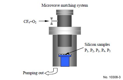
Figure 1: The down-stream plasma etching system.
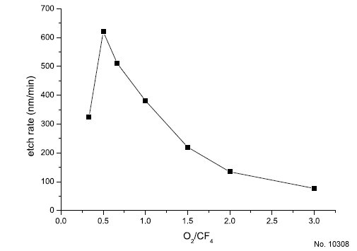
Figure 3: The relation between etch rate and flow rate ratio of O2 and CF4.
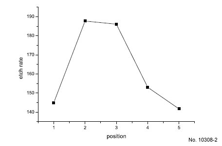
Figure 4: The etch rate distribution along the diameter direction of the holder.