Alphabetical Index
Browse by Elements
Keyword Search
Dry Etchants
Dry and Wet Etchants
Wet Etchants
Bulk Etchants
Layer Etchants
Nano Etchants
Single Crystal Etchants
Thin Film Etchants
Thin Foil Etchants
Wafer Etchants
Al Etchants
Cd Etchants
Ga Etchants
Ge Etchants
In Etchants
New Etchants
Other Etchants
Si Etchants
Zn Etchants
Help
Home
Si Wafer - Wet Etching
Material Name: Si
Recipe No.: 10312
Primary Chemical Element in Material: Si
Sample Type: Wafer
Uses: Etching
Etchant Name: None
Etching Method: Wet etching
Etchant (Electrolyte) Composition: The technique involves minimal equipment, most of
which is readily available. The only specialized equipment is
a photoresist spinner, a contact mask, and a thermal oxidation
furnace. Other equipment includes ovens for soft and
hard baking of photoresist, an alignment fixture for holding
the mask in contact with the wafer, a temperaturecontrollable,
heater-jacketed Pyrex bath with a water-cooled
lid, magnetic stir bars, a hot plate/stirrer, and various Pyrex
and Teflon beakers capable of holding the wafers. The materials
required include (110) lightly doped silicon wafers
rhp >=0.1 Ogm x cm, photoresist, photoresist developer, hydrofluoric
acid (HF 50% in H2O), ammonium fluoride (NH4F 40% in H2O), concentrated sulfuric acid (H2SO4), 30% hydrogen
peroxide solution (H2O2 that is not stabilized is preferred,
stabilized H2O2 contains tin), potassium hydroxide (45%
KOH by weight in H2O), and isopropyl alcohol.
When reading this procedure, there are a few items to
keep in mind. First, any mention of water for mixing solutions
or rinsing means deionized H2O. For mixture recipes,
the proportions are volumetric, unless otherwise stated. Finally,
after each step involving an aqueous mixture, the wafers
should be rinsed in deionized H2O for 5 min then blown
dry with a moisture-free and oil-vapor-free gas.
A photomask of the desired pattern is needed for pattern
development on the masking layer. The one used here is
designed for trench production, and consists of 1.041 cm by
0.512 cm die patterned in chromium. Each die consists of 74
sets of five trenches, with 5, 10, 15, 20, and 30 mm widths.
They are separated by 10 mm lines that are the silicon walls
after processing. The trenches and walls are aligned with the
0.512 cm direction. Eight test patterns are dropped in around
the periphery and in the center of the wafer for quantification
of the etch process ~see Fig. 1!. Dimension tolerance, photoresist
exposure, wafer orientation marks, and 66 sets of
trenches make up the features of the diagnostics die.
The first step is to create the masking material on the
cleaned silicon wafers. A thermally grown oxide or nitride is
required. The layer needs to be thick enough to last until the
end of the second KOH etching step. A 7600 Å wet silicon
oxide layer is grown at ~1000 °C on 3-in. (7.5 cm)-diam
boron-doped (110) Si wafers. To estimate the thickness of the
masking layer required, the observed oxide etch rate in the
KOH baths is abut 10 Å/min. Including all process steps, a
1000 Å would have been sufficient in this example. The
silicon:silicon dioxide etch selectivity for the entire process
is about 3000:1.
Once the masking layer is grown, it needs to be patterned.
Shipley 1813 photoresist is applied to the wafer, then it is
spun at 3500 rpm for 30 s. The wafer is then softbaked at
95 °C for 30 min. After the photoresist is softbaked, the wafer
is mounted in the mask alignment fixture. The fixture
consists of two aluminum frames that can be tightly clamped
together. On one-half of the fixture there is an opening so
that the photomask is fixed in it with epoxy mounting seals.
The tolerances between the alignment pins and fixture holes
should be as small as possible to minimize slippage. The
wafer should be oriented such that a 35.3° counterclockwise
angle between the wafer flat and the desired patterned mask
lines is formed. This is a critical step, since the degree of
misalignment determines the amount of anisotropy achieved,
and the microscopic roughness of the sidewalls. A tolerance
of 62° is found to be adequate for the process, though alignment
within 61° is routinely achievable. When the fixture is
clamped together, the photoresist should be in contact with
the photomask everywhere on the wafer. Any gaps will lead
to poor image registration. The wafer is then exposed to the
ultraviolet (UV) light source. Exposure time will have to be
determined for each process, but the exposure used in this
case is 26 s for a Model 23 Optical Associates light source in
a Model 750 Optical associates mask aligner. It is important
to make sure the wafer is at a constant distance from the light
source to minimize exposure variation.
Photoresist developing is done in a 5:1 H2O: Shipley 351 Microposit developer for 45 s. (The developer is a NaOH,
surfactant, H2O mixture.) It is hardbaked at 140 °C for 30
min. After this coating, a backside coating of photoresist is
applied with another hardbake. The backside coating is used
to preserve the back side oxide. The wafer is then placed in
a buffered oxide etch (BOE) for 10–11 min, or until the
wafer becomes hydrophobic, to etch through the oxide masking
layer. A HF:NH4F 1:11 solution is used to inhibit swelling
and liftoff of the photoresist. The photoresist is then
stripped in a Piranha etch of concentrated H2SO4:30% H2O2
at 6:1, heated to 120 °C. (Depending on the hydrogen peroxide
temperature and age, it may not be necessary to apply an
external heat source.) It is recommended that the hydrogen
peroxide be refrigerated when not in use to prolong its lifetime.
The solution will turn yellowish once the wafer is
added to the solution, but will become clear once the photoresist
is fully removed. A thin oxide layer will form on the
silicon during the photoresist strip, so it is necessary to place
the wafer in the BOE for 30 s to remove the layer.
The next two steps are the most critical of the fabrication
process: the two KOH etches. The temperature tolerances are
very tight, because the etch rate can vary by more than 5000
Å/min within a 10 °C range. Therefore it is recommended
that a 61 °C tolerance be maintained. The first etch is 45%
KOH by weight in H2O heated to 80 °C. The solution is
placed in a heat jacketed Pyrex bath with stirring capabilities.
The bath needs to be covered to minimize fluid evaporation.
A water-cooled lid is recommended for fluid retention.
Stirring of the solution needs to be active enough to keep the
solution thoroughly mixed to minimize thermal and concentration
gradients ~120–150 rpm!. Place the wafers in the bath
only after it has reached its proper temperature. The etch rate
is about 3 mm/min with a typical anisotropy of 150:1. After
the etch the trench sidewalls have been formed. The sidewalls
are perpendicular to the face of the wafer after this
etch, but between the bases and the sidewalls are slanted
faces that are parallel to the (311) plane and protrude about
20 mm from the sidewall (see Figs. 1(a) and 1(b)).
The second etching step uses a 25% by weight KOH in
H2O. The purpose of this etch is to remove the slanted faces
at the bottom of the trench. Once the KOH solution is in the
bath, a 5 cm layer of isopropyl alcohol is added to it. The
alcohol forms an immiscible layer on top of the KOH solution.
The alcohol can be mixed into the KOH by stirring at
about 120–150 rpm. The alcohol boils at 84 °C, so it is critical
that the bath always be kept below this temperature,
though the operating temperature of this bath is 8061 °C.
The bath needs to be stirred such that the alcohol layer is
mixed with the H2O. Wafers need to be spaced such that they
receive adequate circulation of the solution. The etch rate is
2500 Å/min, but the anisotropy is only 6:1 (see Fig. 2). This
etch attacks the slanted faces very effectively, and completely
removes them within 5–10 min. Longer etching risks
overetching in the lateral direction.
The last step is to remove the remaining masking oxide.
Typically 10–15 min in the BOE solution will suffice. The
wafer is rinsed for 5 min in H2O and then blown dry. After
this step the process is complete (see Fig. 3).
Figure 1 shows the effects of the 80 °C KOH, H2O etch
on (110) Si with the (111) aligned masking layer. The trench
walls are perpendicular to the (110) plane, and the etch rate
is about 2.5 µm/min. For the sample shown in Fig. 1(a), the
anisotropy is about 150:1, however, the trenches have slanted
bases. Other samples show trenches as deep as 40 µm, with
widths of 5 µm. Examining Fig. 1(b), in which there is more
than 100 µm between the walls, it can be seen that the slanting
face does not intersect the (110) plane. By measuring the
angles between the (111) and (110) planes with the slanting
plane, it is seen that the slant is about 32° from the (110), and
about 58° from the (111) face. This coincides with the (31T1)
plane intersecting the (111), and (1T0) planes. These slanting
layers are also seen for closely spaced grooves etched into
(110) silicon by Bean and Kendall. Also, the ends of the
trenches have been etched into other planes. The plane of the
ends of the trenches is (112).
Figure 2 shows the effect of the KOH/H2O/isopropyl alcohol
etch on another wafer. The sidewall etching is much
more pronounced, and the anisotropy is about 6:1 with an
etch rate of about 2500 Å/min. However, the most important
feature to note is the absence of the slanted plane. It is not
possible to see the slanted plane under any magnification.
The etch rate of this process is similar to that measured by
Price under similar conditions.
By combining the two etches, it is possible to get the best
features of both etches. The KOH/H2O etch is applied to
create the trench, with KOH/H2O isopropyl alcohol to remove
the slanted plane at the bottom. The result of the twostep
etch is shown in Fig. 3. The overall process anisotropy
is about 50:1 for the silicon. Of course this will vary to some
degree depending on the relative etching times of the two
solutions. One problem encountered during etching is that
the 5 µm trenches experienced a slightly lower etching rate
of about 3%. This is probably caused by poor fluid transport
within the trench. It should be noted, however, that poor
stirring during the second etch will destroy the patterned
features. Therefore, spacing of the wafers in the bath and the
degree of mixing must be carefully adjusted and maintained.
Procedure (Condition): No data
Note: A simple technique for creating trench structures in silicon using readily available wafer processing
techniques is discussed. By using orientation dependent etching of ~110! Si, it is possible to create
trenches in silicon with vertical sidewalls. The etching anisotropy of certain solutions used with this
technique is greater than 600:1 [110]:[111] etching, making it possible to fabricate virtually any
value of aspect ratio trench. For this technique, which makes use of two etchants, an anisotropy
of 50:1 is demonstrated. The equipment, materials, and processing steps required are
outlined.
Reference: Jeremy A. Theil, Deep trench fabrication by Si (110) orientation dependent etching, J. Vac. Sci. Technol. B 13(5), Sep/Oct 1995, pp. 2145-2147.
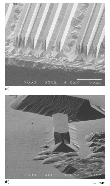
Figure 1: (a) Scanning electron microscopy secondary electron image of
etched trenches using 80° 45% KOH in H2O for 5 min. (b) Scanning electron
microscopy secondary electron image of etched mesas using 80° 45%
KOH in H2O for 5 min.
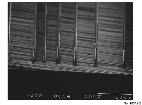
Figure 2: Scanning electron microscopy secondary electron image of etched
trenches using 80° 25% KOH in H2O and isopropyl alcohol for 120 min.
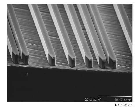
Figure 3: Scanning electron microscopy secondary electron image of etched
trenches using a combination of the two etchants, each for 5 min.