Alphabetical Index
Browse by Elements
Keyword Search
Dry Etchants
Dry and Wet Etchants
Wet Etchants
Bulk Etchants
Layer Etchants
Nano Etchants
Single Crystal Etchants
Thin Film Etchants
Thin Foil Etchants
Wafer Etchants
Al Etchants
Cd Etchants
Ga Etchants
Ge Etchants
In Etchants
New Etchants
Other Etchants
Si Etchants
Zn Etchants
Help
Home
Nano-Fabrication of 30 nm Size MTJ - Silicon - Dry Etching
Material Name: Silicon
Recipe No.: 10313
Primary Chemical Element in Material: Si
Sample Type: Wafer
Uses: Etching
Etchant Name: None
Etching Method: Dry etching
Etchant (Electrolyte) Composition: See the data file.
Procedure (Condition): No data
Note: No data
Reference: Bernardo José Calmeiro Pires, Sub-100 nm Spintronic devices on large area wafers, MSc Thesis, Technico Lisboa, 2016, pp. 6, 10.
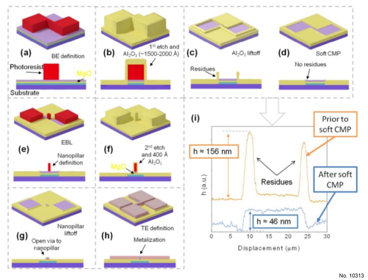
Figure 1: Layout of the nano-fabrication process. (a) BE definition by using optical lithography. (b) Stack full
etch and passivation with a thick Al2O3 layer. (c) Oxide lift-off leaving residues. (d) Removal of oxide residues
using a soft CMP step. (e) Nano-pillar definition and pads protection using EBL. (f) Second etch in two steps and
passivation with a thin Al2O3 layer. (g) Opening of the via to the nano-pillar by oxide lift-off. (h) TE definition by
optical lithography and metallization. (i) Profilometer scans of BE following the thick oxide lift-off (c) and after being
submitted to a soft CMP step (d) to remove lift-off residues.
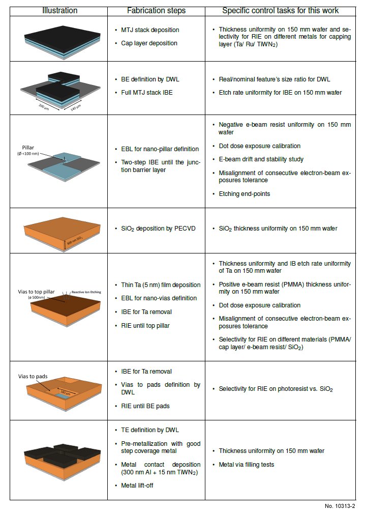
Figure 2: Nano-fabrication of 30 nm size MTJ in 150 mm wafer using RIE approach to open via to pillar.