
Alphabetical Index
Browse by Elements
Keyword Search
Dry Etchants
Dry and Wet Etchants
Wet Etchants
Bulk Etchants
Layer Etchants
Nano Etchants
Single Crystal Etchants
Thin Film Etchants
Thin Foil Etchants
Wafer Etchants
Al Etchants
Cd Etchants
Ga Etchants
Ge Etchants
In Etchants
New Etchants
Other Etchants
Si Etchants
Zn Etchants
Help
Home
TiN Metal Hardmask - Wet Etching
Material Name: TiN
Recipe No.: 10317
Primary Chemical Element in Material: Ti
Sample Type: Layer
Uses: Etching
Etchant Name: None
Etching Method: Wet etching
Etchant (Electrolyte) Composition: Residue removal experiments were conducted in beakers at
45ºC for 2 minutes. The residue removal efficiency was
evaluated from SEM results (Hitachi S-5500) in the areas of
etched sidewalls, via bottoms and on the tops of the wafer.
The Cu etch rate experiments were conducted at 30 °C and
40 ºC and Cu experiments were at 30 ºC, 40 ºC and 55 ºC; each
experiment was 10 minutes in duration. TiN etch rate
experiments were conducted at 30 °C for 10 minutes, 40 ºC for
7 minutes and 55 ºC for 5 minutes. The etch rates were
calculated as the difference in thickness, before and after,
divided by the chemical treatment time. The TiN, Co and Cu
thicknesses were measured using a Four Point Probe Meter
333A. The TEOS, low-k and SiON etch rate experiments were
conducted at 30 °C, 46 ºC and 55 ºC for 10 minutes each. The
TEOS thickness was measured with KLA-Tenor SM300. Lowk
and SiON material thicknesses were measured with Auto SE
Spectroscopic Ellipsometer by HORIBA JOBIN YVON.
The hydrogen peroxide used for HCX-T002C formulation
was semiconductor grade PURANAL (Aldrich 40267), and
semiconductor grade hydrogen peroxide by VWR (JT2190-3)
was used for the HCX35 series formulation study.
The test for Cu oxidation barrier functionality was
conducted by first removing CuOx from Cu blank wafer pieces
with an in-house procedure. Then the Cu wafer pieces were
treated with the experimental product under study: HCXT002C
at 50 ºC, HCX35 at 55 ºC or HCX35-1 at 55 ºC, each
for 2 minutes followed by a 5 minute deionized water (DIW)
rinse and dry. Another Cu blank wafer piece with CuOx
removed was used as a control, with the only treatment being a
5 min DIW rinse and dry. SEM was used to examine the CuOx
growth on all three Cu blank wafer pieces.
Fig. 1 shows that the TiN etch rate is increased with
increasing H2O2 concentration at 30 ºC and pH 9.2. In the
absence of hydrogen peroxide the TiN etch rate is zero. H2O2
is used to oxidize TiN to permit removal of TiN. The low Cu
etch rate (<2 Å/min) shown in Fig. 1 is due to the presence of
the Cu corrosion inhibitor which prevents Cu from being oxidized and subsequently removed during the process. Fig. 2
shows that the TiN etch rate is increased with “compound A”
concentration at 45 ºC. In the absence of “compound A”, the
TiN etch rate is about 62 Å/min. With 1.5% “compound A” in
the formulation the TiN etch rate is nearly doubled. To further
enhance TiN/Cu etch rate selectivity, another novel TiN etch
enhancement component, “compound B”, was added to a
formulation containing 1% of “compound A”. The resulting
TiN etch rate is increased with “compound B” concentration at
45 ºC as shown in Fig. 3. Fig. 2 and 3 show a low Cu etch rate
overall (<2Å/min), and that “compound A” and “compound B”
have no impact on Cu etch rate at 45 ºC.
Fig. 4 shows the TiN and Cu etch rates versus pH at 45 ºC
for formulations containing 1% “compound A”. The TiN etch
rate increases with increasing pH because the etch rate is
directly related to HO2- species concentration. As the pH
increases, the concentration of HO2- also increases, resulting in
a higher TiN etch rate. Fig. 4 also shows that the TiN etch
rate can be tuned by simply adjusting the pH. To obtain a
constant TiN etch rate while maintaining H2O2 concentration
unchanged, it is important to keep pH unchanged. The Cu etch
rate remains very low (<2 Å/min) throughout the pH range
studied due to the presence of the copper corrosion inhibitor.
Metal etch rates of various formulations are shown in Table 1. By increasing process temperature from 30 to 40 ºC, the TiN
etch rate of HCX-T002C is increased from 30 Å/min to 65
Å/min. HCX35a with 1.5% “compound A” shows a higher
TiN etch rate (250 Å/min) vs. the TiN etch rate of HCX35
with 1% “compound A“ (200 Å/min), however, the Cu etch
rate is excessive for HCX35a, and the formulation is not
compatible with Cu. HCX35-1 with 1% “compound A” and
5% “compound B” shows a 233 Å/min TiN etch rate and a low Cu etch rate (<2 Å/min).
Fig. 5 illustrates (via SEM) two progressions of TiN
etching with process time at 55 ºC. In the first (Fig. 5 a-c),
HCX35 creates the TiN pullback after 60 seconds and complete
TiN removal after 120 seconds. In the second (Fig. 5 d-f),
HCX35-1 creates a significant TiN pullback after 30 seconds,
and complete TiN removal after 90 seconds. After 60 seconds
process time the TiN mask is almost completely removed by
HCX35-1 compared with HCX35 which shows only the TiN
pullback morphology in the same amount of time.
The effect of various formulations on the dielectric material
etch rates are shown in Table II, which highlights the low
impact of formulations on low-k, SiON and TEOS dielectrics.
Fig. 6 shows the etching residues after dry etching using
TiN as an etching mask. Fig. 7 shows the complete removal of
these etching residues after treatment with HCX-T002C at
45ºC for 2 minutes, and also shows the TiN pulled-back
morphology.
The SEM in Fig. 8 and 9 show the effect of the formulas on
copper oxidation. Fig. 8(a) shows that CuOx [3] was re-grown
after a 5 minute DIW rinse and dry. Fig. 8(b) and Fig. 9(a) and
(b) show that there are no CuOx formations after Cu was
treated with HCX-T002C, HCX35 and HCX35-1 respectively,
demonstrating that all three formulas have the ability to prevent
CuOx growth.
The formula, HCX-T002C, with a TiN/Cu etch rate
selectivity of more than 60 has been developed. The formula is
compatible with Cu, Co, low-k, TEOS and SiON dielectric materials and is able to remove all etching residues. This
formula prevents Cu oxidation during and after cleaning,
thereby relaxing queue-time restrictions between cleaning and
subsequent process steps.
HCX-T002C is ideal for applications that benefit from TiN
mask pullback morphology. HCX35 and HCX35-1
formulations with TiN/Cu etch rate selectivity greater than 200
have been developed. These formulations are compatible with
Cu, low-k, TEOS and SiON materials, and prevent Cu
oxidation during and after cleaning. The etch residue cleaning
performance of these formulations are currently under study.
Procedure (Condition): No data
Note: Formulations with TiN/Cu etch rate selectivity
greater than 60 at 40 °C for TiN pullback and 200 at 55° C for
complete TiN mask removal, respectively, have been developed.
The formulations are compatible with Cu, low-k and SiON
materials, and prevent Cu re-oxidation.
Reference: Hua Cui, TiN Metal Hardmask Etch Residue Removal with
Mask Pullback and Complete Mask Removal for Cu Dual Damascene Device, ASMC 2012, pp. 305-307.
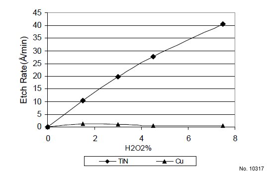
Figure 1: TiN and Cu etch rate vs. H2O2 % at 30 ºC (pH: 9.2).
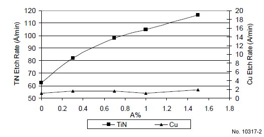
Figure 2: TiN and Cu etch rate vs. comp. A% at 45 ºC (H2O2 fixed,
pH: 8.8).
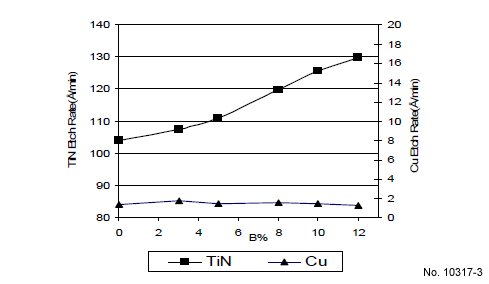
Figure 3: TiN and Cu etch rate vs. comp. B% at 45 ºC (H2O2 fixed,
pH: 8.8).
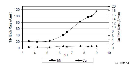
Figure 4: TiN and Cu etch rate vs. pH at 45 ºC.
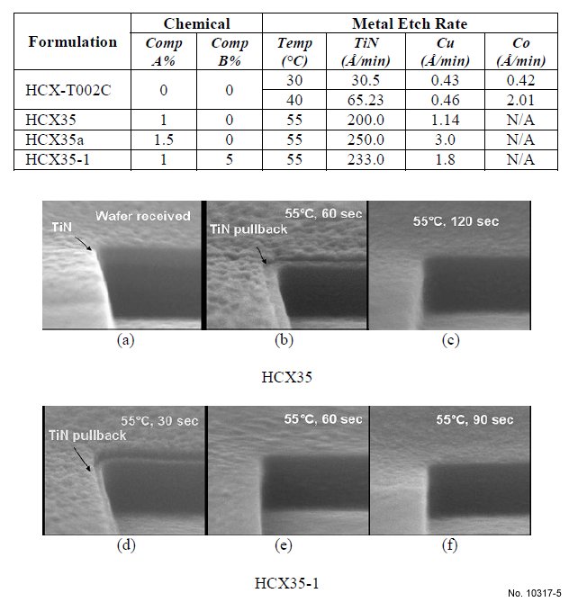
Figure 5: TiN Etch SEM for HCX35 and HCX35-1.
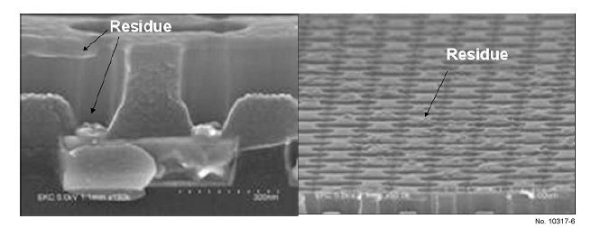
Figure 6: Wafer SEM as received.
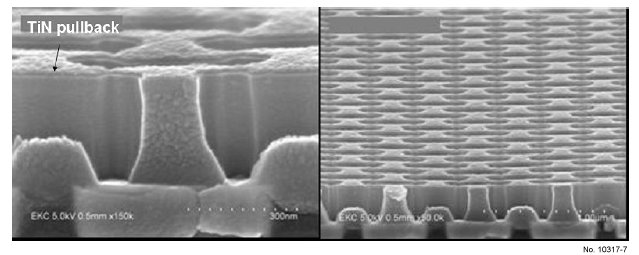
Figure 7: SEM after cleaning at 45 ºC, 120 sec (removed residues,
formed a TiN pullback).
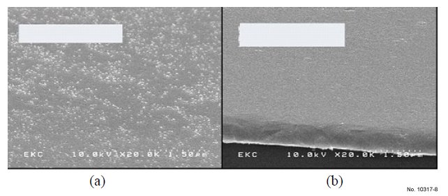
Figure 8: Two Cu coupons with CuOx removed: (a) 5 min DIW rinse
only (b) Treated with HCX-T002C chemical at 50 °C for 2 min and then
5 min DIW rinse.
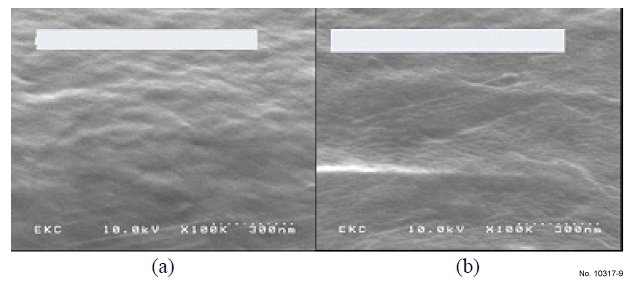
Figure 9: Two Cu coupons with CuOx removed: (a) Treated with
HCX35 at 55 °C for 2 min, then 5 min DIW rinse (b) Treated with
HCX35-1 at 55 °C for 2 min and then 5 min DIWrinse.
Table 1: Etch rate on various dielectric materials.
