Alphabetical Index
Browse by Elements
Keyword Search
Dry Etchants
Dry and Wet Etchants
Wet Etchants
Bulk Etchants
Layer Etchants
Nano Etchants
Single Crystal Etchants
Thin Film Etchants
Thin Foil Etchants
Wafer Etchants
Al Etchants
Cd Etchants
Ga Etchants
Ge Etchants
In Etchants
New Etchants
Other Etchants
Si Etchants
Zn Etchants
Help
Home
CoSi2 Contacts - Wet Etching
Material Name: CoSi2
Recipe No.: 10320
Primary Chemical Element in Material: Co
Sample Type: Layer
Uses: Etching
Etchant Name: None
Etching Method: Wet etching
Etchant (Electrolyte) Composition: To study cobalt silicide formation between Co films and heavily
doped poly-Si for low contact resistance contacts, very thin (target
thickness of ~20 nm) Co films were sputtered on heavily P+ implanted
(~60 nm thick) poly-Si/SiO2/Si wafers, followed by a TiN and Ti film
cap layer. Three hundred millimeter (300 mm) p- Si wafers were used
as substrates in this study.
The wafers were annealed to form cobalt silicide in the two types
of RTA systems (the cold wall, tungsten halogen lamp-based RTA
system1 and the hotwall, furnace-basedRTAsystem1) in the
temperature range of 350 ~ 900 C in 1 atm N2 ambient. The residual
O2 concentrationwas kept below 30 ppm during RTA steps. The cobalt
silicide formation process consists of two annealing steps: the first step
at lower temperature, ~500 C, for the higher resistivity monosilicide
(CoSi) formation, and the second step at higher temperature, >800 C,
for the lower resistivity disilicide (CoSi2) formation. The annealing
time was 15 ~ 30 s for the cold wall RTA and 50 ~ 150 s for the
hot wall RTA system. Extensive design of experiment (DOE) utilizing
over 200 samples was implemented. The 'annealing time' refers to
the 'soak time' at annealing temperature for the cold wall RTA system
and the 'residence time' (from wafer-in to wafer-out) in the annealing
chamber for the hot wall RTA system. Details of RTA systems have
been reported elsewhere.
During the low temperature 1st step annealing for CoSi formation,
Co film was partially converted into CoSi with any unreacted Co
film remaining as a metal layer. The TiN/Ti capping layer and the
unreacted Co film were stripped off by chemical etching before the
2nd step annealing, at higher temperature, for CoSi2 formation. TiN
capping layer was removed in a H2O2 + H2O (1:1) solution at 6 0C. The Ti and unreacted Co layers were etched off using a HNO3 + H2O
(1:1) solution at 60 C. Sheet resistance (Rs) was measured at various stages (as prepared,
after 1st step anneal, after metal film strip, and 2nd step anneal) using
a four point probe to characterize the cobalt silicidation process and
the low resistivity CoSi2 formation annealing process optimization.
Procedure (Condition): No data
Note: The effect of annealing temperature and time on the resulting resistivity of CoSi2 contacts with P-doped poly-Si was investigated
using a single wafer furnace-based (hot wall) rapid thermal annealing (RTA) system. To achieve low resistivity contacts, CoSi2
formation process optimization was done by detailed design of experiment (DOE). Sheet resistance (Rs) response surface plots as a
function of annealing temperature and time for 1st step and 2nd step RTA processes showed a very wide process window. The hot
wall RTA resulted in significantly (>20%) lower Rs, over a very wide process window, compared to the equivalent RTA process
using conventional tungsten halogen lamp-based (cold wall) RTA systems. Dopant (P) depth profiling results by secondary ion
mass spectroscopy (SIMS) revealed that the P atoms in the CoSi2 film and at the CoSi2/P-doped poly-Si interface, redistribute very
differently under different RTA conditions. The CoSi2 formation process was optimized utilizing characteristics of P pile-up near
the CoSi2/P-doped poly-Si interface to suppress P depletion from the P-doped poly-Si layer for contact resistance minimization.
Reference: Jin Yul Lee, et al., Towards Contact Resistance Minimization through CoSi2
Formation Process Optimization on P-Doped Poly-Si by Hot
Wall-Based Rapid Thermal Annealing, ECS Journal of Solid State Science and Technology, 4 (7) P220-P225 (2015).
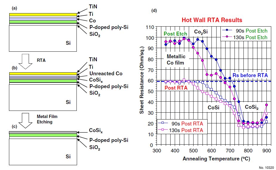
Figure 1: (a) ~ (c) Schematic illustrations of cross-sections of TiN/Ti/Co/P-doped poly-Si/SiO2/Si wafers along process sequences. (d) Temperature and time
dependence of sheet resistance of TiN/Ti/Co/P-doped poly-Si/SiO2/Si wafers annealed in a hot wall RTA system, before and after TiN capping layer and unreacted
Co layer etching.