Alphabetical Index
Browse by Elements
Keyword Search
Dry Etchants
Dry and Wet Etchants
Wet Etchants
Bulk Etchants
Layer Etchants
Nano Etchants
Single Crystal Etchants
Thin Film Etchants
Thin Foil Etchants
Wafer Etchants
Al Etchants
Cd Etchants
Ga Etchants
Ge Etchants
In Etchants
New Etchants
Other Etchants
Si Etchants
Zn Etchants
Help
Home
GaAs - Dry Etching
Material Name: GaAs
Recipe No.: 10322
Primary Chemical Element in Material: Ga
Sample Type: Wafer
Uses: Etching
Etchant Name: None
Etching Method: Dry etching
Etchant (Electrolyte) Composition: All test wafers were taken as 3-inch S.I. GaAs wafers
with thickness ~650 µm. These wafers were then coated
within 30 µm thick positive photoresist AZ 4620 and exposed
to define circular holes with 70 µm diameter. The patterned
photoresist was post-baked at 120°C to improve plasma etch
resistance and adhesion. The patterned wafers were then
mounted on a carrier wafer with wax to make them loading
compatible with ICP system. This is necessary in view of the
fact that ICP etching requires cooling of the wafer during
etching, which is very difficult to achieve without carrier wafer.
GaAs wafers were then etched in standard ICP system,
one at a time. An oxygen plasma de-scum step prior to
etching was utilized in order to remove any residual
photoresist in the hole, which would have otherwise
contributed to the roughness of the etched surface. Plasma of
etcher is inductively coupled through a coil at 13.56 MHz,
with independent energy control provided by 13.56 MHz RF
biasing on the substrate. Helium gas was used to cool
backside of the wafer. The substrate temperature was set at
20 °C for all test conditions. The etch chemistry was a
mixture of Cl2/BCl3 through mass flow controlled process
gas lines. The chamber was evacuated to a base pressure of ~
9 x 10 exp(-6) Torr by a turbo-molecular pump backed by a dry
mechanical pump before initiating the etch process. The etch
gases mixture was introduced through an annular region at
the top of chamber lid. ICP etching was carried out using
positive photoresist mask to etch holes selectively. All the
etching runs were carried out through a design of
experiments by varying ICP power, process pressure,
Cl2/BCl3 flow rate ratio and chuck bias power. The etch rate,
etch depth, etch profile, mask selectivity and surface
morphology of etched features were determined by Scanning
Electron Microscopy (SEM). Deposition on the etched
sidewall was analysed by high resolution Energy Dispersive X-ray Analysis (EDAX).
Effect of Pressure: Fig. (1) shows the variation of etch rate and the undercut
with the process pressure. The process pressure is varied
from 5 mTorr to 12 mTorr at a constant ICP power of 800W,
RF bias power of 8 0W and Cl2:BCl3 ratio of 4:1. It is seen
that the etch rate increases gradually from 4.6 µìm/min to
6 µm /min, when the pressure is raised from 5 mTorr to
12 mTorr. The increase in the etch rate with the pressure is
attributed to an increase in the concentration of reactive
chlorine species that enhances chemical component of the
etching. This suggests reactant limited regime at lower
pressures. In addition, it is evident from the figure that the
undercut also increases from 19.6 µm to 21.5 µm when the
pressure is increased from 5 mTorr to 12 mTorr. The reason
for the enhanced undercut can be understood as follows.
Actually the mean free path and plasma efficiency reduces as
we raise the pressure. This results in a reduction in sputtering
component on the etched surface. The decrease in sputtering
component with increasing pressure results in poor surface
morphology of etched surface with higher undercut. On the
other hand, the etch profiles obtained at the pressure of
10 mTorr and 12mTorr under identical conditions are shown
in Fig. (2). It is clear from the figure that the better surface
morphology of etched surface is achieved at 10mTorr with
slight narrowing at the bottom of etched profile.
Effect of ICP Power: In Fig. (3), we show the variation of etch rate with ICP
power for two different pressures of 10 mTorr and 12 mTorr.
It is obtained here that the etch rate gets increased with the
ICP power up to 600 W at 10 mTorr pressure and 80 W RF
bias power, suggesting that the etching is limited by reaction
rate mechanism. This is attributed to higher concentration of
reactive chlorine radicals, which increase the chemical
etching component and hence ion flux that enhances the
bond breaking and sputter de-sorption efficiency of the etch
process. Further increase in the ICP power (above 600 W)
however leads to a relatively constant etch rate, which is
mainly due to competition between the sputtering and the
etch reaction as a consequence of increased ions that are
sputtering the adsorbed species (neutrals or ions) out of the
surface prior to etch reaction. This sputter de-sorption at
higher ICP powers results in etched surface with better
surface morphology at the same RF chuck bias power.
Fig. (4) shows the etch profile obtained at higher ICP
power of 1000 W, when the pressure is kept as 10 mTorr.
Under this situation, the etch profile with smooth etched
sidewalls is obtained. Fig. (3) also shows that the reaction
limited regime is enhanced up to 800 W with an increase in
the process pressure to 12mTorr at 60 W RF bias power.
Further, as the concentration of reactive species is increased
with pressure, their sputter de-sorption at 600 W is not
sufficient to remove active species. Hence, the etch rate is
found to saturate after 700 W up to 1000 W at 12 mTorr and
60W RF bias power.
Effect of RF Bias Power: The dependence of etch rate and mask selectivity on the
RF bias power is shown in Fig. (5). It is clear from the figure
that the etch rate depends strongly on the bias power and it
gets enhanced rapidly from 4.73 µm/min to 5.36 µm /min,
when the bias power is increased from 60W to 90W. These
observations were made at 800 W ICP power, 10 mTorr
pressure and 4:1 as the Cl2:BCl3 ratio for 15 min as the etch
time. Enhancement in the etch rate is mainly attributed to
higher physical etching component at higher bias power due
to enhanced sputtering as a result of increased ion energy,
which improves removal of etch by-products and assists in
bond breaking. In addition, the etch an-isotropy is found
to enhance as RF bias power is increased. This is expected as
the ion energy gets increased due to the higher DC bias,
which leads to the straight sidewall profile of the etched
feature.
The GaAs: photoresist etch selectivity was determined by
the ratio of GaAs etch rates to photoresist etch rates. This is
portrayed in Fig. (5), where photoresist selectivity shows a
strong dependence on the RF bias and ICP power. Mask
selectivity is found to deteriorate from 15.53 to 13.85 when
the bias power is increased from 60 W to 90 W. This is
mainly caused by enhanced physical etching component at
higher RF biases. It would be worth mentioning that this is
one of the best reported selectivity using photoresist mask
for GaAs etching applications at low pressures. The increase
of resist etch rate with RF bias power and ICP power is due
to dominant physical etch mechanism. Actually larger RF
bias power increases the energy of ions bombarding the
wafer surface and the higher ICP power increases the density
or flux of the ions bombarding the wafer surface. Both of
these activities finally enhance the physical etch mechanism.
On the other hand, the reduced resist etch rate with
increasing pressure is mainly due to less physically and
higher chemically driven processes as a result of increased
reactant concentration at higher pressure.
The desired etch profile with controlled side wall angles
and surface smoothness can be obtained with a proper
balance between enhanced sputter de-sorption of etch byproducts
and surface protection by by-products. The sputter
de-sorption of etch by-products is a function of ion energy
that depends upon pressure and ICP/bias power. Based on
above experimentation we arrived at a optimum recipe with
ICP power of 800 W, bias power of 60 W and pressure of
12 mTorr that resulted in etch profile with smooth surface
and controlled sidewalls with angle of ~84º, without
narrowing at the bottom, as shown in Fig. (6).
The straighter sidewall at the bottom is perhaps due to
the balanced chemical and physical etching components at
800 W ICP and 60 W RF bias. The EDAX spectrum of
optimum etched surface, as shown in Fig. (7), also indicates
negligible deposition of CClx polymer, most probably due to
a better balance between enhanced sputter de-sorption of
etch by-products and surface protection by by-products.
Moreover, the etched GaAs surface roughening is strain
induced, which tends to be more at defect sites due to
higher strain that leads to non-uniform etching.
Etch Rate Variation with Cl2: BCl3 Flow Rate Ratio: Fig. (8) shows the etch rate variation with Cl2/BCl3 flow
rate ratio in ICP plasma for an etch time of 60 min at the
pressure of 15 mTorr. Here we observe that the etch rate is
increased from 2.3 µm/min to 2.7 µm/min as the flow ratio is
enhanced from 3 to 6.5. This is mainly due to an increase in
chlorine radicals with increasing percentage of Cl2 in gas
mixture that is responsible for chemical etching. Etch byproducts
staying on the surface block the fresh enchant
species from reacting. This saturates the etch process and
eventually leads to a reduction in etch rate at the above ratio
of Cl2:BCl3 as 6.5. In other words, above 6.5 ratio, reactant
limited regime dominates that reduces the etch rate. This
behavior suggests that the balance between physical etching
component and chemical etching component gets
deteriorated with the flow rate ratio, which degrades the
surface smoothness. On the other hand, the de-sorption of
chemical species limits the etching process at higher Cl2 flow
rates, leaving some of the residue on the surface itself.
This is shown in Fig. (9).
The EDAX spectrum of etched surface clearly indicates
the deposition of CClx polymer at high flow rates and
pressures (Fig. 10), which would have otherwise sputtered
away at low pressures due to higher ion energy.
Effect of Etch Time: Fig. (11) shows the dependence of average etch rate and
etch depth on the etch time for ICP power of 800 W, 12 mTorr pressure and 60 W bias power. The average etch rate
is found to decrease with etch time, from 5.26 µm/min at an etch depth ~ 79..m to 1.71µm/min at an etch depth ~ 162..m.
This is mainly due to the reduction in the effectiveness of
supplying reactive species and removal of etch by-products
with increased depth. The etch rate reduction can be
compensated by increasing the gas flow rates and pressure.
However, this in turn results into deeper etch profiles with
severe by-product deposition on the sidewalls. This makes it
necessary to incorporate a polymer cleaning process for
deeper profiles after completion of etching step.
Procedure (Condition): No data
Note: GaAs etch characteristics like etch rate, etch profile sidewall angle, etch surface morphology and selectivity are
studied as a function of Inductively Coupled Plasma (ICP) power and Cl2/BCl3 flow rate ratio in ICP at low pressure
(<15mTorr) and low RF bias power (<100W) regime to achieve moderate GaAs etch rate with an-isotropic profiles and
smooth surface morphology. The low pressure regime etching at Cl2/BCl3 flow rate ratio of 4:1 has resulted in vertical
etch profiles with controlled sidewall angle ~84 deg., smooth surface morphology and good mask selectivity ~15 without
significant deposition of CClx polymer on the etched sidewalls but with limited etch depth ~ 100 µm using photoresist
mask. The mask selectivity is found to be a strong function of RF bias power and ICP power and a weaker function of
process pressure. The resultant etch depth increases with an increase in pressure and flow rate ratio at the expense of etch
surface morphology, as the desorption of chemical species limits the etching process at higher Cl2 flow rates and leaves
some of the residue on the surface.
Reference: D.S. Rawal, et al., A Highly Selective Low Pressure Inductively Coupled Plasma Etching
Process for GaAs Using Photoresist Mask, The Open Plasma Physics Journal, 2011, 4, 34-39.
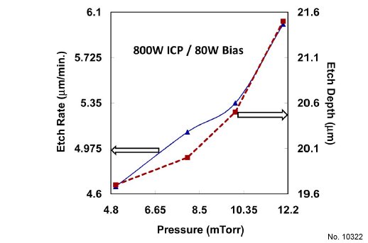
Figure 1: Variation of etch rate and undercut with the pressure.
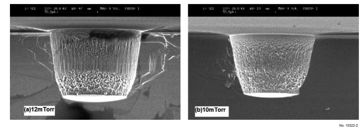
Figure 2: Etch profiles obtained under identical conditions at the pressure of (a) 12 mTorr and (b) 10 mTorr.
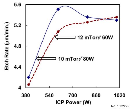
Figure 3: Variation of etch rate with ICP power.
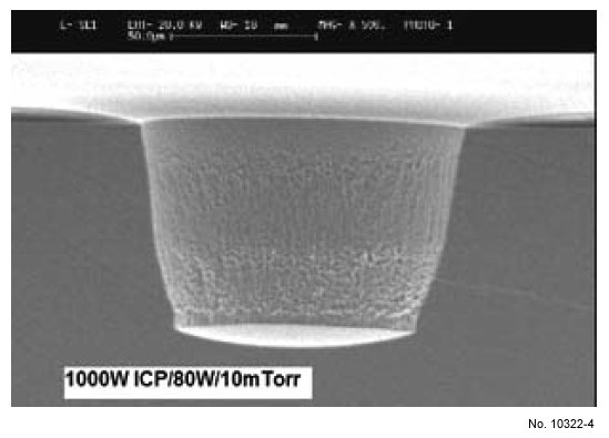
Figure 4: Etch profile obtained at 10 mTorr pressure.
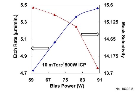
Figure 5: Dependence of etch rate and mask selectivity on RF bias
power.
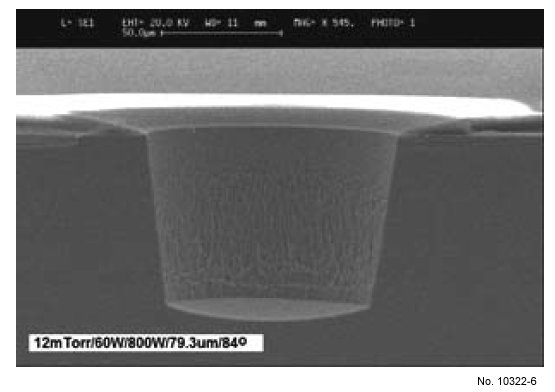
Figure 6: Optimum etch profile with smooth surface morphology
and controlled sidewall angle of ~84º.
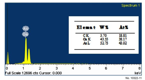
Figure 7: EDAX spectrum of etched surface at 12mTorr pressure,
800 W ICP and 60 W RF bias.
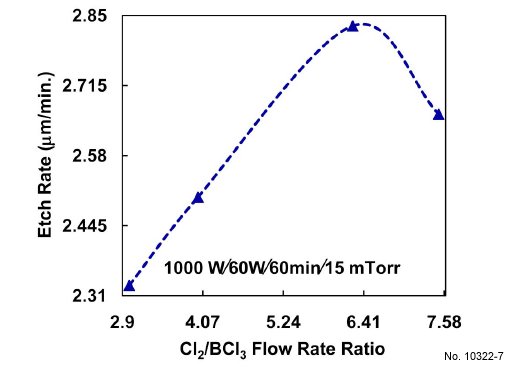
Figure 8: Etch rate variation with Cl2/BCl3 flow rate ratio at
15 mTorr/1000 W ICP/60 W RF bias.
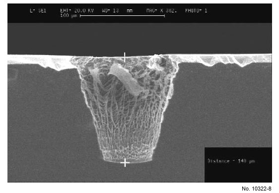
Figure 9: Etch profile obtained at 15m Torr with Cl2= 125 sccm and
BCl3= 20 sccm flow rates and 1000 W ICP/60 W RF bias.
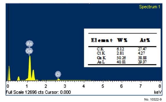
Figure 10: EDAX spectrum of etched surface at high gas flow rates.
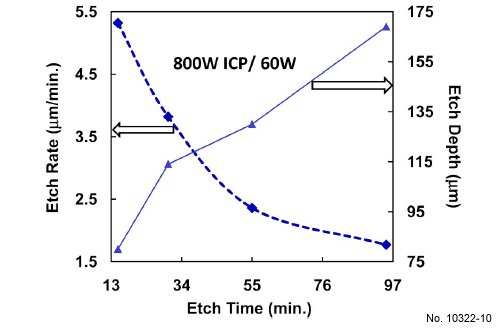
Figure 11: Dependence of average etch rate and etch depth variation
on etch time.