Alphabetical Index
Browse by Elements
Keyword Search
Dry Etchants
Dry and Wet Etchants
Wet Etchants
Bulk Etchants
Layer Etchants
Nano Etchants
Single Crystal Etchants
Thin Film Etchants
Thin Foil Etchants
Wafer Etchants
Al Etchants
Cd Etchants
Ga Etchants
Ge Etchants
In Etchants
New Etchants
Other Etchants
Si Etchants
Zn Etchants
Help
Home
ZnSe - Wet Etching
Material Name: ZnSe
Recipe No.: 10329
Primary Chemical Element in Material: Zn
Sample Type: Wafer
Uses: Etching
Etchant Name: None
Etching Method: Wet etching
Etchant (Electrolyte) Composition: The research was carried out using crystal wafers of
undoped ZnSe(I) (without thermal annealing), ZnSe(II) (after thermal annealing) and doped ZnSe(Al) and ZnSe(Te) crystals grown by the Bridgman method.
Chemical modification of the II-VI semiconductor
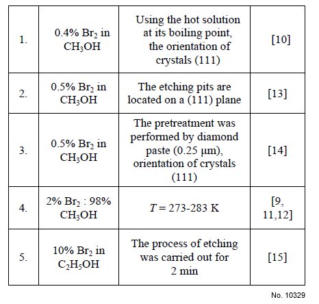
compounds surfaces is often carried out using bromine
containing mixtures. To obtain more perfect polished surface of ZnSe crystals, bromine containing
etching compositions such as Br2 in methanol or
ethanol with different bromine content has been used (Table 1).
Mechanical polishing the samples. Polishing: ZnSe(I), ZnSe(II), ZnSe(Al), ZnSe(Te) plates after
cutting by our developed method should be performed
using abrasive powder with grain sizes M 10, M 5 and
M 1, or diamond powders ASM 28/20, ASM 10/7,
ASM 5/3, ASM 3/2, ASM 2/1 and ASM 1/0. The
polishing mixture is prepared in the form of abrasive
powders aqueous suspensions with distilled water. The
process should be carried out on a glass grinder,
alternately treating the plate with both sides within 1-
5 min by each abrasive (in order to decrease abrasive
grit) depending on the thickness of the damaged layer
that must be removed. After this, the samples should be
thoroughly washed with warm distilled water using the
addition of a small amount of detergent, then several
times with distilled water and dried in air. The
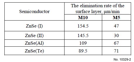
elimination rate of the surface layer was different
depending on the nature of these materials and abrasive
grit (Table 2). The ZnSe(Al) material elimination rate
was 6 µm/min when we made polishing by abrasive
diamond powders ASM 28/20, and by powder ASM 5/3
amounts to 4 µm/min. For ZnSe(Te) crystals the surface
layer elimination rate with abrasives ASM 28/20 is equal
to 18 µm/min and 2 µm/min with diamond powder ASM 5/3.
Chemical-mechanical polising: Elimination of the surface damaged layer should be carried out using the
CMP method. To make the CMP process for ZnSe(I),
ZnSe(II), ZnSe(Al), ZnSe(Te) samples, we developed
polishing solution at a volume ratio of components:
10 H2O2:10 HBr:80 EG characterized by small etching
and high polishing ability. We recommend holding the
etching mixture for 2 hours in order to achieve the
maximum concentration of free bromine, which is
formed during interaction of etching components. The
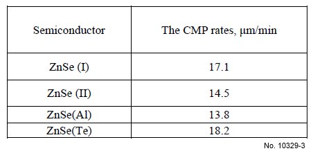
CMP process of wafers that are prepared in etching
solution with the rate 2 ml/min was carried out for 5 min
at T = 298 K using a cambric tissue covered glass
polisher, and CMP rate do not exceed 20 µm/min (Table 3).
Inter-cleaning the ZnSe surface after each stage
of treatment: After each stage of mechanical treatment
carried out surface inter-cleaning of undoped and doped
ZnSe single crystals should be made for removing dirt
from the surface of plates produced during cutting,
grinding and mechanical polishing. At first, to remove
the physical or mechanical contamination (dust, abrasive
particles, metallic materials and semiconductor crumbs,
which are formed during grinding) by rinsing in distilled
water with addition of surface-active substances.
Removing organic contaminants (grease, glue, residues,
suspension, and fingerprint) was conducted by
degreasing in organic solvents (ethanol, acetone), after
which the crystals should be thoroughly dried in flow of
purified air before the following technological
operations.
Procedure (Condition): No data
Note: The process of chemical polishing the undoped and doped ZnSe crystals
surface with H2O2 – HBr etchants has been studied. The dependence of the samples
polishing rate on the concentration of H2O2 in HBr solution has been investigated.
Surface states after chemical etching have been established using electron and atomic
force microscopies, and it was shown that the surface state is improved after chemical
etching. Etchant selection to develop slow polishing compositions for chemicalmechanical
polishing the investigated materials has been made. Concentration regions of
polishing solutions have been found for various types of ZnSe surface treatment: to
remove the damaged layer, to control the etching rate, to obtain samples of a given
thickness.
Reference: V.Ì. Tomashyk, et al., Optimization of conditions for treatment of ZnSe crystal surfaces
by chemical etching, Semiconductor Physics, Quantum Electronics & Optoelectronics, 2013. V. 16, N 2. pp. 140-145.
Table 1: The etchant compositions for chemical treatment
of ZnSe crystals.

Table 2: The elimination rates of ZnSe crystals surface
layer during mechanical polishing by free abrasives.

Table 3: The CMP rates of undoped and doped ZnSe
crystal surfaces.

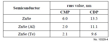
Table 4: Surface roughness of undoped and doped ZnSe
after chemical treatment in the new bromine emerging
etchants.
