Alphabetical Index
Browse by Elements
Keyword Search
Dry Etchants
Dry and Wet Etchants
Wet Etchants
Bulk Etchants
Layer Etchants
Nano Etchants
Single Crystal Etchants
Thin Film Etchants
Thin Foil Etchants
Wafer Etchants
Al Etchants
Cd Etchants
Ga Etchants
Ge Etchants
In Etchants
New Etchants
Other Etchants
Si Etchants
Zn Etchants
Help
Home
TiN - Wet Etching
Material Name: TiN
Recipe No.: 10332
Primary Chemical Element in Material: Ti
Sample Type: Thin film
Uses: Etching
Etchant Name: None
Etching Method: Wet etching
Etchant (Electrolyte) Composition: Test vehicles consisted in HfO2/TiN film stacks deposited in 100 nm
deep nanotrenches and 200 nm deep cylindrical nanoholes.
Nanotrenches were etched in a 100 nm thick polySi film, using a 10 nm
SiO2 etch stop layer on a Si wafer. Trench CD was 31–35 nm, with a
pitch of 90 nm. Trenches were covered with 1.5 nm HfO2 and 25 nm
TiN deposited by ALD (atomic layer deposition). Nanoholes were
manufactured using a sacrificial nanopillars scheme. First 200 nm-tall nanopillars were etched in Si wafers
with a pitch of 90 nm and a diameter of about 40 nm, as described
in [6]. The diameter of the Si pillars was decreased by steam oxidation.
Then the space between the pillars was filled with silicon dioxide by
PEALD (plasma-enhanced ALD). The oxide overburden was removed by
a STI-like CMP stopping on the Si pillars. Finally, the Si pillars were
back-etched using a timed wet TMAH etch. The obtained nanoholes had
a top diameter varying from 11 to 27 nm, as shown in the SEM picture
in Fig. 2. Finally, the nanoholes were covered with HfO2/TiN films similarly
to the nanotrenches.
Etch tests were performed on coupons in beakers using APM 1:4:20
at 65 °C or room temperature (RT), adapting the etch rate to the layer
thickness to enable a kinetic analysis. To avoid any influence of the
presence of air-oxidized TiN at the surface of the TiN films on the results
of a kinetic test, a 2 min dilute HF (0.5%v) etch was performed at RT just before the APM etch.
Procedure (Condition): No data
Note: In the manufacturing of multi-Vt FinFET transistors, the gate material deposited in the nano-spaces left by the
removed dummy gate must be etched back in mask-defined wafer areas. Etch conformality is a necessary
condition for the control of under-etch at the boundary between areas defined by masking. We studied the
feasibility of TiN etching by APM (ammonia peroxide mixture, also known as SC1) in nano-confined volumes
representative of FinFET transistors of the 7 nm node and below, namely nanotrenches with 1-D confinement
and nanoholes with 2-D confinement. TiN etching was characterized for rate and conformality using different
electron microscopy techniques. Etching in closed nanotrenches was conformal, starting and progressing all
along the 2-D seam, with a rate that was 38% higher compared to a planar film. Etching in closed nanoholes
proved also to be conformal and faster than planar films, but with a delay to open the 1-D seam that seemed to
depend strongly on small variations in the hole diameter. However, holes between the fins at the bottom of the
removed dummy gate, are not circular and do present 2-D seams that should lend themselves for an easier start
of conformal etching as compared to the circular nanoholes used in this study. Finally, to explain the higher etch
rate observed in nano-confined features, concentrations of ions in nanoholes were calculated taking the overlap
of electrostatic double layers (EDL) into account. With negatively charged TiN walls, as measured by streaming
potential on planar films, ammonium was the dominant ion in nanoholes. As no chemical reaction proposed in
the literature for TiN etching matched with this finding, we proposed that the formation of ammine complexes,
dissolving the formed Ti oxide, was the rate-determining step.
Reference: Guy Vereecke, et al., Wet etching of TiN in 1-D and 2-D confined nano-spaces of FinFET
transistors, Microelectronic Engineering 200 (2018) 56–61.
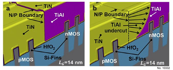
Figure 1: nMOS first process simulation of an N7 bulk FinFET. The shown cross-section is along a shared 14 nm gate at the n/p boundary after TiAl etch using either (a)
a fully anisotropic or (b) a fully isotropic etch. In (b) the n/p boundary undercut reaches the proximity of the first fin of the nMOS.
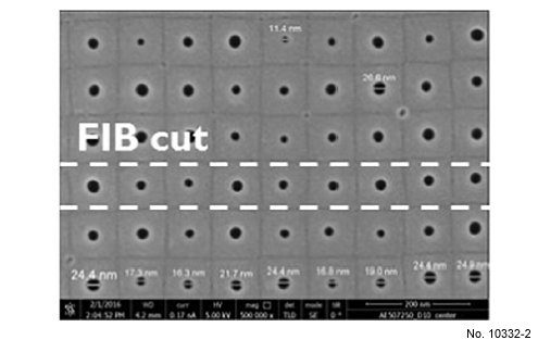
Figure 2: Top-down SEM view of nanoholes before HfO2 and TiN deposition,
showing the variability of holes' diameter and a FIB cut lamella for TEM inspection.
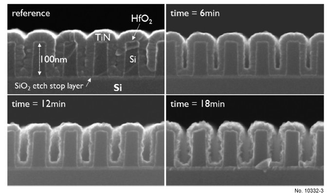
Figure 3: X-SEM of the nanolines test structure covered with 1.5 nm HfO2 and 25 nm TiN at different times of etching by APM 1:4:20 at RT after a 2 min dilute HF (0.5%
v) etch at RT.
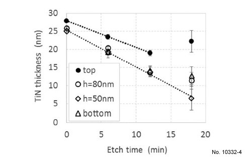
Figure 4: Summary of TiN etch test on filled nanolines using APM 1:4:20 at RT,
showing the higher etch rate in-between nanolines as compared to the top.
Dotted lines are the linear regression lines for the data sets at top and 50 nm
above trench bottom.
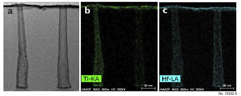
Figure 5: Pictures of nanoholes covered with 5 nm TiN on 1.5 nm HfO2 after 3 min etching in APM 1:4:20 at RT after a 2 min dilute HF (0.5%v) etch at RT: (a) TEM, (b)
Ti EDS map, (c) Hf EDS map. The diameters at the top were 12.6 nm and 15.3 nm, for the left and right hole, respectively.
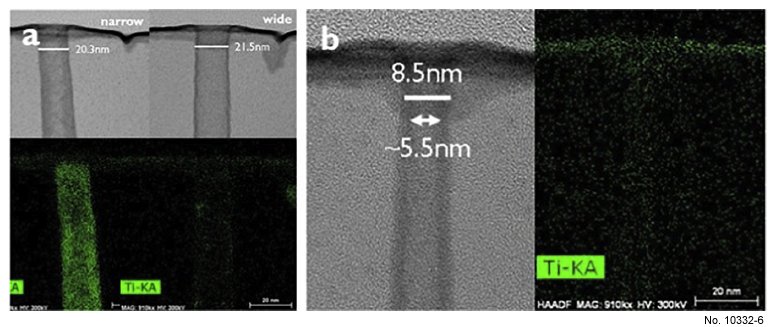
Figure 6: TEM pictures and Ti EDS maps of nanoholes filled with 10 nm TiN on 1.5 nm HfO2 after etching in APM 1:4:20 at 65 °C for 30 s (a) and 1.5 min (b), after a
2 min dilute HF (0.5%v) etch at RT.