Alphabetical Index
Browse by Elements
Keyword Search
Dry Etchants
Dry and Wet Etchants
Wet Etchants
Bulk Etchants
Layer Etchants
Nano Etchants
Single Crystal Etchants
Thin Film Etchants
Thin Foil Etchants
Wafer Etchants
Al Etchants
Cd Etchants
Ga Etchants
Ge Etchants
In Etchants
New Etchants
Other Etchants
Si Etchants
Zn Etchants
Help
Home
Sub-Micrometer Trenches in Silicon - Dry Etching
Material Name: Silicon
Recipe No.: 10333
Primary Chemical Element in Material: Si
Sample Type: Wafer
Uses: Etching
Etchant Name: None
Etching Method: Dry etching
Etchant (Electrolyte) Composition: Bosch process etching: The basic Bosch process is a time-multiplexed plasma etch process typically involving three distinct steps that alternate - depassivation, etch and repassivation. Some steps maybe performed concurrently. To overcome the problem of excess bowing at the top of the trenches and of narrowing at the bottom, numerous etch trials accompanied by a detailed study of the relationship between the three etch steps were performed. The best etch profile was obtained using a two-step process in which the depassivation and the etching were
combined in one step. Since silicon etching takes place in this
case at a lower pressure than in the regular Bosch process, this
leads in a decrease of both etch rate and selectivity. Two sets
of experiments were performed with the optimized Bosch
process. Set 1constitutes simple trench test structures of 800
nm width, whereas Set 2 consists of trenches increasing in
width from 250 nm to 5ìm, with spacing of ~250nm between
them. Both were fabricated on standard <100> p-doped silicon
(Ultrasil – resistivity 0.01-0.015 Ohm x cm). The detailed etch
programs used for the two experiments are shown in Table 1,
and the obtained results are represented in Figure 1. Using the
Set 1 etching conditions in Table 1, 800 nm-wide trenches with
extremely vertical profiles and no bowing were manufactured,
reaching aspect ratios as high as 124:1 (Figure 1a). As feature
size decreases, achieving high aspect ratios becomes easier.
Being able to achieve a ratio of 124:1 on trenches as wide as
800 nm-wide trenches is therefore a challenge, requiring
dynamic adjustments of both the duration of the steps and of
the plasma power for Set 1. The previous HAR record of
107:1 was obtained on 374 nm-wide structures using Set
2 etch parameters, which, by extrapolating data from Figure 3,
would result in an aspect ratio of approximately 80:1 if
applied to 800nm structures. Using the Set 2 etch conditions
in Table 1, the highest aspect ratio was obtained for the 250
nm-wide trenches. The etch extended 40 µm in depth, resulting
in an extremely high 160:1 aspect ratio. The post-etch dicing
of the samples for the purpose of SEM observation resulted in
collapsed walls, as apparent in Figure 1b, however the
effectiveness of etch is apparent from the regular square
profile at the bottom of the trenches, which also suggests that
even higher aspect ratios might be possible by further etching.
Cryogenic DRIE: By comparison with the Bosch process, cryogenic DRIE
offers the benefit of producing highly vertical sidewalls with
no scalloping effect, which are of great s ignificance when
etching sub-micrometer structures. This is a consequence of
the process being carried out at extremely low temperatures,
and results in reduced isotropic etching of silicon.
The challenge in case of cryogenic etches is to use a suitable
mask that will resist at such temperatures and that can be
patterned at sub-micrometer length scales. For the final set of
experiments performed in this work (Set 3), we used a
combination of focused ion beam (FIB) etching and cryogenic
DRIE to achieve HAR trenches with widths in the tens of
nanometers range. The FIB was used to pattern lines of 35+/-
10 nm width and 500 nm spacing on a 70 nm-thick aluminum
film. This created a hard mask for the subsequent etching,
which used the process parameters shown in Table II. Figure
2 shows the corresponding SEM results, indicating that aspect
ratios of >125:1 could be achieved. We also note that the FIB
was used again, before the imaging, to etch a vertical
rectangular hole that exposes a partial cross-sectional view of
the etching. We would like to explicitly mention that these are
preliminary results and that further work is ongoing.
Procedure (Condition): No data
Note: This paper focuses on Deep Reactive Ion Etching (DRIE) of sub-micrometer features. Very high aspect ratios up to 160:1 on trenches of 250 nm have been achieved using the Bosch process and 120:1 on 35 nm-wide trenches using a cryogenic process. The proposed etch recipes are specifically optimized for sub-micrometer features, and are not compatible with feature sizes in the tens of micrometer range. Based on analyzing data from our experiments and from literature, we show that a previously reported two-parameter empirical logarithmic law accurately describes the dependency of aspect ratio on trench width over a wide range of widths and etch parameters, including the sub-micrometer regime. We also propose a new figure of merit that describes the ultimate aspect ratio achievable for any given etch process.
Reference: Jayalakshmi Parasuraman, et al., Very High Aspect Ratio Deep Reactive Ion Etching of Sub
micrometer Trenches in Silicon, JMEMS-2012-0181, pp. 1-4.
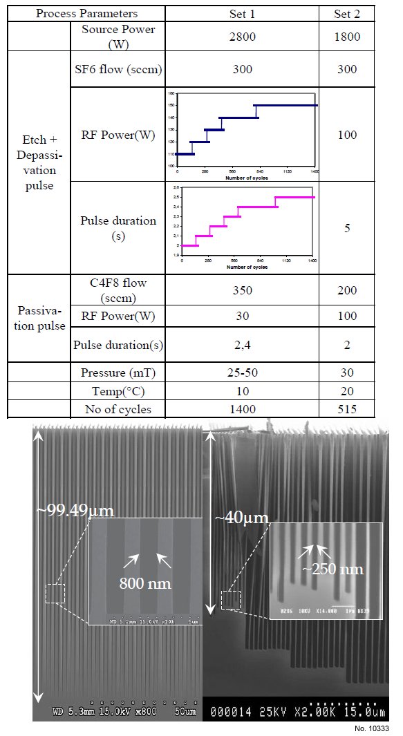
Figure 1 + Table 1: Table 1: Parameters for deep etching of sub-micron features. Figure 1: HAR structures manufactured using the Bosch process: (a) 800nmwide
trenches with a depth of 99.5 µm (aspect ratio 124:1) and (b) 250 nm - wide trenches with a depth of 40 µm (aspect ratio 160:1). Some of the walls
collapsed during the dicing procedure.
Table 1: Process parameters for the cryogenic etch process (Set 3).
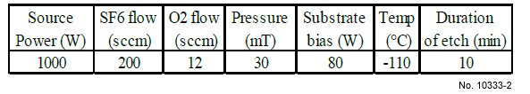
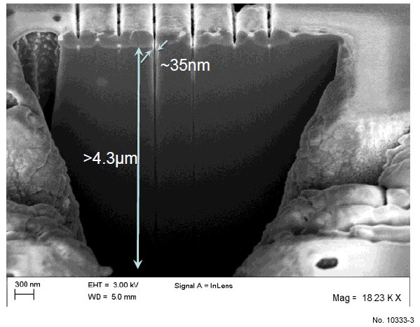
Figure 2: SEM image of ~35 nm trench etched to a depth greater than 4.3 µm,
hence with aspect ratio >125:1. A rectangular hole was etched using the FIB
to allow cross-sectional visualization.