Alphabetical Index
Browse by Elements
Keyword Search
Dry Etchants
Dry and Wet Etchants
Wet Etchants
Bulk Etchants
Layer Etchants
Nano Etchants
Single Crystal Etchants
Thin Film Etchants
Thin Foil Etchants
Wafer Etchants
Al Etchants
Cd Etchants
Ga Etchants
Ge Etchants
In Etchants
New Etchants
Other Etchants
Si Etchants
Zn Etchants
Help
Home
3D Charged Particle Trap - Dry Etching
Material Name: Silicon
Recipe No.: 10335
Primary Chemical Element in Material: Si
Sample Type: Wafer
Uses: Etching
Etchant Name: None
Etching Method: Dry etching
Etchant (Electrolyte) Composition: An Oxford Plasmalab 100 machine (Oxford Instruments
plc, Abingdon, Oxfordshire OX13 5QX United Kingdom)
was used for DRIE. The machine has RF plasma power of up
to 30 0W at 13.56 MHz, ICP power of up to 3000 W at
13.56 MHz, and a substrate temperature range from -150 to 400 C. Helium flows across the back side of the wafer at
2–10 sccm to maintain a constant pressure of 10 Torr. The SF6 flow ranges from 50 to 300 sccm, while the O2 flow rate
ranges from 5 to 40 sccm. For RIE, a South Bay Technology RIE 2000TM was used. It has an RF power range of 0–20 0W at a frequency of
13.56 MHz. It can reach a base pressure of 1 x 10 exp(-5) Torr and offers highly anisotropic etching with minimal undercutting.
Photoresist mask for silicon dioxide etching: A 0.004-mm oxide layer was grown thermally on Si
(front and back) by using a wet oxidation method. The hole pattern was transferred to the wafer using the photolithography
process described previously. Wet etching of an oxide resulted in an undesirable oxide
profile at the hole edges, as shown in Fig. 6. The AZ5214TM
photoresist (Clariant Corp., AZ Electronic Materials) was
ultimately used as the mask. The exposed oxide was etched in a buffered oxide etch solution.
Several different photoresists were tried as masks for
oxide etching, including AZ5214 (Clariant Corp.), SU8
2025TM (MicroChem Corp.), PR1-4000ATM (Futurrex,
Inc.), and SU8 2010TM (MicroChem Corp.). AZ5214 and
PR1-4000 A, being positive photoresists, had poor RIE selectivity
and developed poor sidewall profiles. These two
materials were not used as oxide etch masks. SU8 2025
photoresist is widely used for MEMS applications because
of its robust nature. This photoresist develops with vertical
profiles and has high selectivity to oxide. Better results
were obtained using SU8 2025 in RIE, but other problems
arose. SU8 2025 is a highly viscous photoresist and often
formed bubbles when applied to the wafer. These bubbles
had to be removed by using a pipette. We finally used SU8
2010, which has a much lower viscosity than SU8 2025. It
was easier to remove the bubbles from this photoresist
while maintaining high oxide selectivity during the RIE process.
During photolithography with the SU8 photoresist, we
also used OmniCoatTM by MicroChem, which allowed easy
stripping of the SU8 photoresist after the oxide mask had
been etched in the RIE process. OmniCoat was spun on the
wafer at 2000 rpm for 30 s and then baked at 200 C on a
hotplate for 1min. Then, the SU8 layer was spun on top of
the OmniCoat layer at 2000 rpm for 30 s. This wafer was
then baked on a hotplate at 65 C for 1 min, followed by a
2-min bake at 95 C. However, the spinning of SU8 2010
led to the formation of edge beads. These edge beads were
thicker and took more time to treat than a thinner and more
uniform layer of SU8. The edge beads adhered to the glass
mask when it was pressed against the wafer during the UV
exposure step. To prevent this, the baking time was
increased to 2.5 min at 95 C. This cured the edge bead
problems.
The problem of bubbles in the viscous SU8 2010 also
caused issues in Si etching. During photolithography, these
bubbles exposed the oxide to RIE, and they were consequently
etched in DRIE. Because larger features etch faster
in DRIE, the bubbles that were larger than 0.1 mm etched
through the wafer faster than the desired 0.1 mm holes. This
problem was solved by using SU8 2005, which is less viscous
than SU8 2010. The SU8 2005 was spun at 1000 rpm
for 30 s and was then soft baked at 65 C for 2 min and at
95 C for 5 min. The SU8 was then exposed to UV light
through the glass mask shown in Fig. 3.
SU8 is a negative photoresist, and thus, we used a mask
opposite to that shown in Fig. 3. The mask was mostly transparent,
while the holes and trenches were opaque. An SU8
layer ~0.010 mm thick requires 110–140 mJ/cm2 of energy
from the UV lamp, according to the product datasheet. A
postexposure bake was then performed with 2min of baking
at 65 C, 3 min of baking at 95 C, followed by another
minute of baking at 65 C. Finally, the wafer pattern was
developed by immersion in the SU8 developer, for 3min for
SU8 2010, and then 2 min for SU8 2005. The exposed oxide
areas were then ready to be etched by RIE.
The following were the optimal RIE parameters for
oxide etching with a SU8 2010 mask: pressure=150 mT, RF power=150 W, CF4 flow=30 sccm, O2 flow=2 sccm,
and duration=1 h.The results of the oxide etch are shown in Fig. 7. The image shows that some of the silicon was also etched during
RIE. This overetching was reduced by simply shortening the etch duration.SU8 was stripped by immersing the wafer in Remover
PGTM heated at 100 C for ~20 min.
Masks for Si etching: Both negative and positive photoresists used in throughwafer
deep etching tend to crack at cryogenic temperatures.
Silicon oxide is a commonly used hard mask for cryogenic
etching and has been used heavily in this research. Metal
masks were also used in this research but were found to be not
quite ideal, although they have a much higher selectivity.
We used a chromium (Cr) thin film metal hard mask
because of its higher selectivity to silicon in DRIE. Also,
growing 0.004 mm of oxide by oxidation can take up to 5
days, while metal film sputtering takes only a few hours. We
performed wet etching of a Cr film and the results were not
uniform, with irregular Cr pieces found in many places.
These irregularly shaped metal masks led to nonuniform
etching of Si around the feature boundaries, as seen around
the hole top and the island in Fig. 8.
There were also unsatisfactory results when using the Cr
lift-off process instead of the Cr wet etch. This was because
of a thin metal film on top of the photoresist, which came
into contact with the metal layer during deposition. This
caused a ripping effect during lift-off, as shown in Fig. 9 and
explained schematically in Fig. 10. This effect resulted in a
rough edge on the metal hard mask in Fig. 9 (the holes
shown in this figure were from an early mask design with
0.5-mm-diameter holes). These rough edges created undesirable
distortions in the hole profiles.
To reduce this ripping effect, we used a bilayer lift-off process
by MicroChem Corp. Lift-Off Resist (LOR 10BTM) is a photoresist composed of a 0.002-mm sublayer below another
positive resist, S1813TM, as shown in Fig. 11. This sublayer
produced a gap between the metal on the photoresist and that
on the wafer, which resulted in clean edges during the lift-off
process.
We used a wafer with a Cr mask and LOR bilayer lift-off
for deep reactive ion etching. In the wafer holes, we noticed
similar levels of bowing to those produced with the oxide
hard mask wafers. These metal masks accumulated negative
charges, which led to the deflection of ions, causing bowing
near the hole tops.
The oxide mask was deemed to be superior because of
the simplicity of the patterning process and because of the
mask’s ability to keep the DRIE chamber free of contamination.
It also prevented unwanted materials from being in the
final trap. Ultimately, purchasing Si wafers with 0.004 mm
oxide layers reduced the time spent on the basic task of Si
wafer wet oxidation.
In choosing between oxide and metals for the hard mask
materials, it was found that the metal masks displayed a
micromasking phenomenon. In the literature, they have been
shown to be an inappropriate material for clamping rings because they become polarized in active plasmas because of
their high conductivity. Self-sputtering led to the local transfer
of small amounts of metal atoms on the wafer, causing micromasking
of the silicon that affected the etch process.
Selection of an etching technique for DRIE: Both the Bosch and cryogenic DRIE processes were
tested on the wafers, but the cryogenic version was chosen
over the Bosch process because of the following negative
characteristics of the Bosch process:
(1) It produced scalloping on the sidewalls (i.e., lines in
saw-tooth form) because of the alternating etching and
passivation cycles that are characteristic of this process.
An example of scalloping is shown in Fig. 12. Smooth
wafer sidewalls are required for the trap operation.
(2) It has low selectivity between the oxide and Si. A thicker
hard mask would be required to etch the holes completely
through 0.5 mm of Si.
(3) Metal masks like Cr and Al can be used for the Bosch
technique, but they have some disadvantages. As discussed
earlier, the metals exhibit a micromasking phenomenon
caused by the self-sputtering of the metal
films. The lift-off process for metal masks is challenging
because in the Bosch process, the feature size depends
largely on the LOR development time. Further calibration
of the development time is required to obtain better
feature size resolution. Metals can also act as contaminants
in the DRIE chamber and the positron traps.
Therefore, Al masks cannot be used in the Bosch technique
to solve the low selectivity issue between oxide
and Si.
(4) The Bosch process creates a fluorocarbon polymer during
the passivation cycle. This polymer forms a layer
inside the ICP tube and the DRIE chamber. This can produce
random changes in the etch rates and the etching
angles.
(5) If cryogenic and Bosch etching are performed alternately,
the DRIE chamber must be cleaned after each
etch. The chamber has to be heated from ~95 C to
room temperature and brought up to atmospheric pressure.
This wastes valuable resources, including liquid
nitrogen and time.
DRIE method selection: Effects of temperature,
pressure, ICP, RF power, gas flow, and O2 gas
percentage on the etching results: Initially, the etching we carried out was based on a method
suggested by Craig Ward of Oxford Instruments. We optimized
his method to produce nearly vertical, smooth sidewalls with
minimum amounts of bowing and crystallographic effects. A
base reference method was achieved for future comparison.
This etch method had a process temperature of ~95 C, pressure
of 12 mTorr, total gas flow of 76 sccm (SF6 þ O2), O2 percentage
of the total gas flow of 7.9%, RF power of 3 W, and
ICP power of 700 W. Figure 13 shows an SEM image of a hole
profile produced while using these etch variables.
After this base result was established, each parameter was
altered while observing the resulting changes in the hole profile.
Major changes were observed in the hole profile with
increases in chamber pressure and temperature, as shown in
Table 1.
As shown in Fig. 14, a higher pressure (14 mTorr)
removed the sidewall roughness and a higher temperature
(~90 C) produced straighter sidewalls (89.8 deg.). Both parameters
were chosen for the final method. This method results
in high aspect ratios for the through-wafer holes with smooth
and near-90 deg. sidewalls.
Figure 15 shows a sample image of the final results when
using the new variables. A small amount of bowing has been
deemed acceptable for trap construction and can be removed
by grinding and polishing. With this final method, holes
were etched through Si wafers and the process has been
reproduced. Etched dies were later stacked axially and
bonded using a thermocompression bonding technique.
These bonded dies allowed the fabrication of one section of
the trap assembly process.
Challenges of cryogenic DRIE through-wafer etching: Several of the complications and issues faced during the
etching of anisotropic, high aspect holes in silicon wafers were associated with use of DRIE at cryogenic temperatures
with an oxide hard mask. These problems were addressed by
changing the process parameters of the DRIE machine. The
issues encountered in this research were bowing, notching,
undercutting, crystallographic plane features, variations in wafer
thickness, DRIE plasma variations, and contamination issues.
Bowing: Bowing is the convex sidewall shape near the hole top
shown in Fig. 16. Boufnichel et al. attributed bowing to
the multiple reflections of ions with incident trajectories that
were not normal to the wafer surface and deflection of ions
on the mask side slopes, which then sputter the passivation
layer at the top. Radicals penetrate through voids created in
the SiOxFy layer and assist the ions in the destruction of the
hole profile. Changing a few of the process parameters
enabled reduction of the bowing effect. When stacking and aligning hundreds of Si wafers axially, it is desirable to have
straight and identical sidewalls in all wafers, without any
deformations in their profiles. Another solution to remove
the bowing effect is to polish off the top of the wafer.
Notching/footing: Notching and footing occur at the bottom of the etched
hole and the ions affect the oxide at the wafer back. The oxide
is a nonconducting material that accumulates negative charges
on its surface and leads to the deflection of the positive ions in
the plasma. These deflected ions start etching into the Si walls
at the bottom of the hole, as shown in Fig. 16. It may be possible
to prevent notching by using a conducting material at the
bottom of the wafer, so that the conducting material will not
accumulate a charge and deflect the ions. To test this hypothesis,
aluminum (Al) was deposited on the back side of a wafer
as an etch stop, but the Al layer, being only 0.0005 mm thick,
started breaking away faster than the oxide. Also, the thermal
conduction was better on the Al etching surface than on the
oxide, which changed the hole profile. The crystallographic
effect appeared at the bottom of the holes. If the Al backing
remained, the table temperature would need to be increased
by at least 10 C to stop the crystallographic angles (which are
explained later in this section) forming at the hole bottom.
Undercutting: Undercutting is caused by the convex corners of the hard
mask, which are open to ions approaching from wider angles
than those for a feature side. It is difficult to remove an
undercut unless a perfectly 90 deg. hard mask corner is established. However, if the top of the wafer is removed by
polishing to eliminate bowing, then the undercut will be
removed simultaneously.
Crystallographic plane features: At certain temperatures below !90 C, the SF6 gas condensation
increases on the wafer surface. This surge results
in etch rate variation in the different crystallographic orientations
of Si. Crystallographic planes with higher atomic densities
etch more slowly and affect the profile at the hole
bottom. To eliminate this undesired feature, the temperature
must be precisely controlled at ~90 C.
Variations in wafer thickness: To ensure that we etched through the Si in all the holes
across the wafer, it was important that the wafer had a uniform
thickness. Changes in the wafer thickness caused
notching to appear in some hole bottoms. This was caused
by ion deflection by the oxide mask, even though some of
the holes had not etched completely through to the oxide on
the back side. A lower total thickness variation of
<0.0005 mm across the wafer was required to ensure that all
wafer parts etched through completely and simultaneously.
Variations in the DRIE plasma: The DRIE plasma was seen to vary in a concentric ring
pattern across the wafer, and it etched more quickly near the
center. According to Hoekstra et al., the clamping ring
induces a deviation in the electrical field lines in the presheath
and thus produces a deviation in the ion trajectory.
This leads to higher ion concentration in the wafer center.
The DRIE specifications from the manufacturer indicate a
variation of 65% in plasma, leading to the same amount of
variation in the etch depth across the wafer. This specification
was found to be accurate. Considering the variation in
the etch depth, it was necessary to ensure that the oxide on
the back did not break until all features were resolved. This
was accomplished by visual inspection near the end of the
etching routine.
Contamination issues: The DRIE process chamber was contaminated by the
metal masks or by the Bosch process. With the Bosch process,
an unidentified tan powder was found in the chamber,
and this powder was difficult to remove with isopropanol
and cleanroom wipes. Because of this contamination, other
DRIE mask materials for Si were avoided. Even with an oxide
mask and when more than six or seven wafers were
etched without cleaning the chamber, some scratches were
still observed on the wafer table. This caused an increase
in the He flow, which altered the wafer temperature and
produced a hole profile change. This issue was solved by
polishing the table using a Scotch BriteTM 3M No. 96
scouring pad, which produced a smoother aluminum table
for wafer placement.
Trench width calibration: The anisotropic etching rate was highly dependent on the
aspect ratios of the etched features. A lag was found when
etching narrower features. In the initial etches, the mask
design had a trench width that was equal to the diameter of
the holes (0.1 mm). The trenches had a higher etch rate
because they contained more exposed Si, even though they
were the same width as the holes shown in Fig. 17. The trenches thus etched through the wafer before the holes,
causing the samples to separate prematurely inside the
chamber.
In the early stages of the research, the trench features
were eliminated to tune the variables for hole etching only.
When the trench features were added back into the mask, the
width also had to be adjusted. The trench width was calibrated
by using a set of ten lines on a temporary mask. The
line widths ranged from 0.1 to 0.01 mm, with intervals of
0.01 mm. This mask was patterned alongside the holes and
was then etched for 90 min. The trenches were imaged in the
SEM and were compared with the hole etch rate. The etch
rate of the 0.035 mm line width was closest to that of the
holes. Another temporary mask was prepared with 0.035mm
trenches and 0.1mm holes and was patterned and etched.
The 0.035 mm trenches broke through before the holes were
completely etched. The alignment holes (shown and marked
in Fig. 3) toward the wafer’s outer edge had a lower etch
rate. This was because of the nonuniform plasma mentioned
earlier. The alignment holes toward the outer edge required
wider trenches. Further research is underway to determine
appropriate trench widths so that all features can be resolved
without breaking the oxide. Possible solutions might include
the use of a bare Si wafer on the back of the etch wafer,
which would allow etching to continue until all features are
etched.
BONDED STACKS OF WAFERS: We used plasma-assisted gold (Au) thermocompression
bonding to stack the etched dies. Au thin films were sputtered
on the etched dies. The Au coated dies were then precleaned
and surface activated in an O2 plasma environment
for 60 s. The dies were pressed manually at room temperature
and were then pressed using a manual hydraulic press.
The stack was then heated to 200 C for 20 min and subsequently
ramped down to room temperature. This experiment
yielded a stack of three etched dies, as shown in Fig. 18.
Hole alignment during the bonding process is still to be
resolved. Future work will involve the use of sapphire rods
inserted completely through the alignment holes (of the
order of 0.1 mm in diameter) of all the bonded dies. This is
important because any deviation from the alignment center
may obstruct the charged particle paths during trapping.
Procedure (Condition): No data
Note: Positrons are charged antiparticles that annihilate upon contact with electrons or any form of
matter. Two of the authors (Lynn and Weber) have proposed a new approach to store large
numbers of charged particles such as positrons. The proposed structure consists of thousands of
0.1-mm-diameter holes etched through silicon wafers, which are then stacked axially to form
cylindrical microtubes to store a large number of positrons. The authors used deep reactive ion
etching on the wafers to create the through-holes with smooth and straight sidewalls. To produce
the best possible etching results, they iteratively modified the etching parameters, including the
chamber pressure, temperature, radio frequency power, inductively coupled plasma power, SF6/O2
gas flow, and O2 gas content. These iterations addressed the fabrication issues that were
encountered, such as bowing, notching, undercutting, nonuniform etch rates across the wafer, and
preferential etching along certain crystal planes. The trench widths were calibrated to match the
etch rates between all the wafer features. The final results enabled the etching of through-wafer
vias with straight sidewalls (89.9–90.1 deg.), smooth surfaces, and high aspect ratios (~5:1) with
minimal defects. This paper describes the etching process used to produce these vias.
Reference: Ankita Verma, Joshah Jennings, Ryan D. Johnson, Marc H. Weber, and Kelvin G. Lynn, Fabrication of 3D charged particle trap using through-silicon vias etched
by deep reactive ion etching, J. Vac. Sci. Technol. B 31(3), May/Jun 2013, pp. 032001-1 - 032001-9.
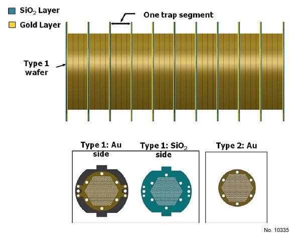
Figure 1: (Color online) Axially stacked wafers contain holes, hence form one
tube with each of the holes.
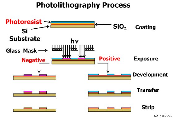
Figure 2: (Color online) Technique of photolithography.
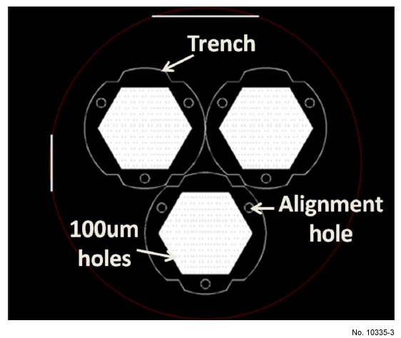
Figure 3: (Color online) Mask used during photolithography.
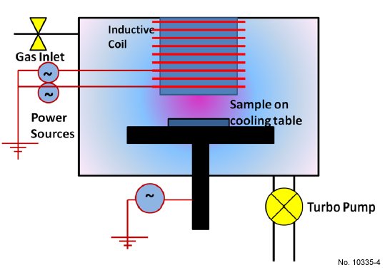
Figure 4: (Color online) Schematic diagram of DRIE with inductive coil which
is not present in RIE.
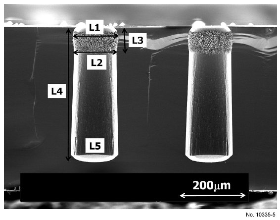
Figure 5: Hole characteristics measured using SEM.
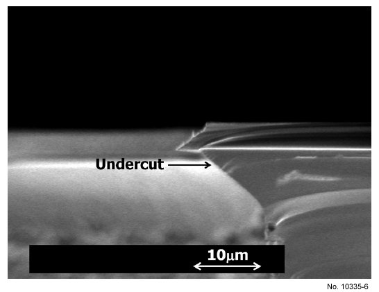
Figure 6: Slanting edges of etched oxide.
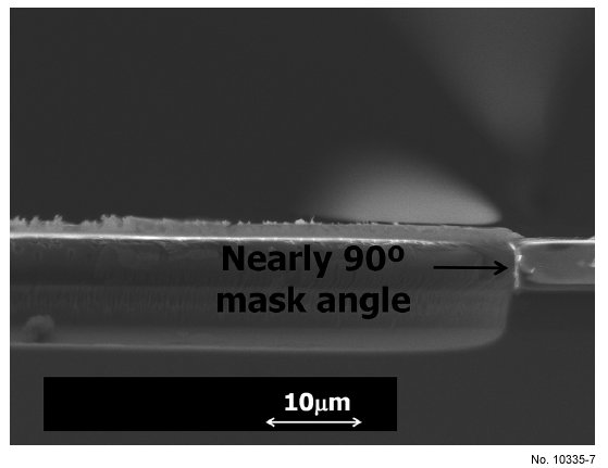
Figure 7: Reactive ion etching result after 1 h of RIE with process pressure of
150 mT, RF power at 150 W, CF4 flow of 30 sccm, and O2 flow of 2 sccm.
Oxide angle after RIE was closer to 90 deg. as compared with earlier attempts
of wet etching.
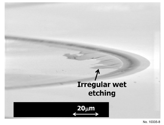
Figure 8: Irregular wet etching of Cr mask.
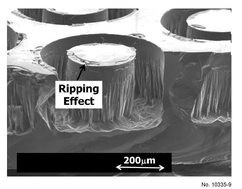
Figure 9: Example of an unsuccessful Cr lift off.
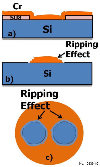
Figure 10: (Color online) Examples of ripping effect: (a) Cr thin film sputtered
on SU8 that is patterned on Si, (b) ripped Cr on Si after lift-off, (c) top view
of wafer after lift off.
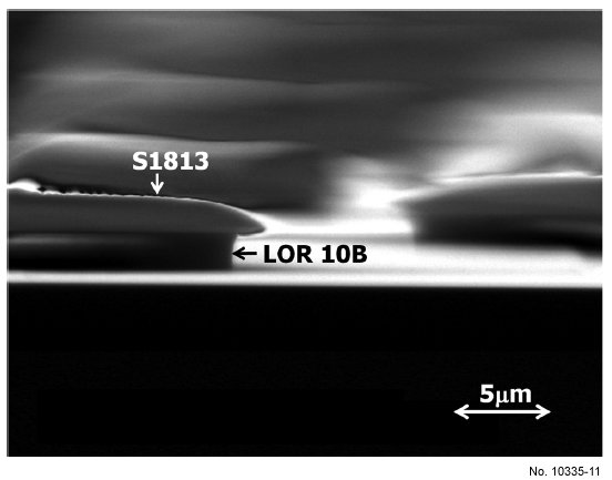
Figure 11: Image bilayer.
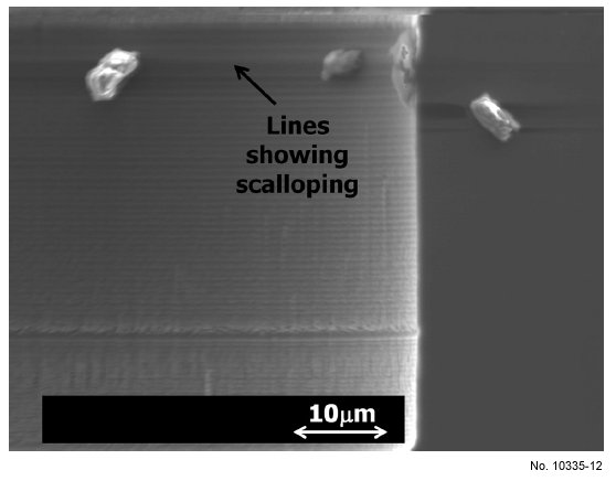
Figure 12: Example of scalloping in Bosch technique. (Dust particles appearing
in the image should be neglected.)
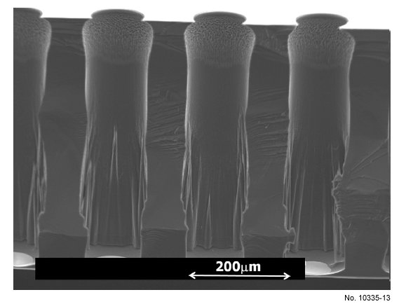
Figure 13: Base etch results in which temperature was ~95 C, pressure was
12 mT, total gas flow (SF6 þ O2) was 76 sccm, O2 percentage in gas was
7.9%, RF power was 3W, and ICP power was 700 W.
Table 1: Results with higher pressure and higher temperature than the base variables after calibration etches.
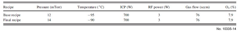
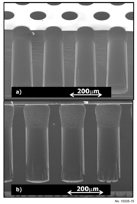
Figure 14: Result of calibration etches: (a) Higher pressure, (b) higher temperature
than base recipe.
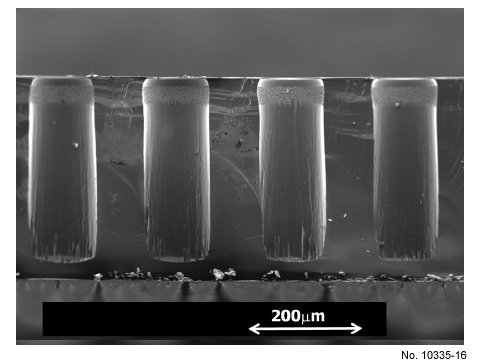
Figure 15: Result of final etch recipe in which temperature was ~90 C, pressure
was 14 mT, total gas flow (SF6 þ O2) was 76, O2 percentage in gas was
7.9%, RF power was 3W, and ICP power was 700 W.
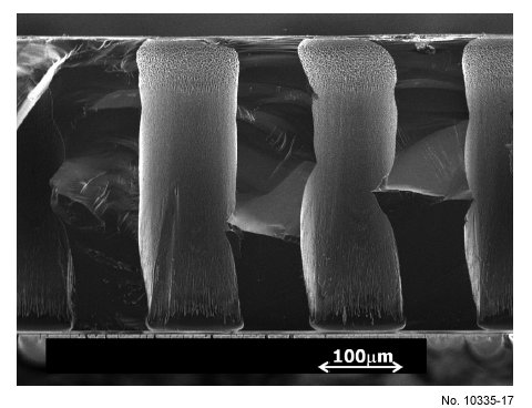
Figure 16: Example of notching and bowing occuring in an etched sample.
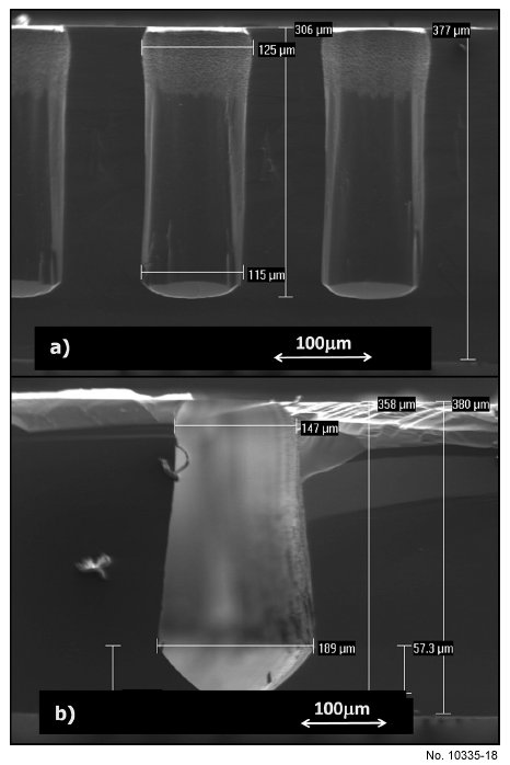
Figure 17: (a) Holes etched 306 µm in 120 min. (b) Trenches etched 358 µm in
120 min.
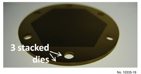
Figure 18: (Color online) Stack of three bonded dies.