Alphabetical Index
Browse by Elements
Keyword Search
Dry Etchants
Dry and Wet Etchants
Wet Etchants
Bulk Etchants
Layer Etchants
Nano Etchants
Single Crystal Etchants
Thin Film Etchants
Thin Foil Etchants
Wafer Etchants
Al Etchants
Cd Etchants
Ga Etchants
Ge Etchants
In Etchants
New Etchants
Other Etchants
Si Etchants
Zn Etchants
Help
Home
SiO2 Nanopillars - Dry Etching
Material Name: SiO2
Recipe No.: 10336
Primary Chemical Element in Material: Si
Sample Type: Nano
Uses: Etching
Etchant Name: None
Etching Method: Dry etching
Etchant (Electrolyte) Composition: Polystyrene (PS)microspheres suspension (2.50 wt. % in water, 500 nm in diameter) was purchased
from Alfa Aesar Corporation (Heysham, UK). The reagents including ethanol, acetone, H2SO4 and NH3.H2O were bought from Sinopharm Chemical Reagent Co., Ltd. (Shanghai, China). 4-ATP and R6G
were obtained from Aladdin Industrial Corporation (Hangzhou, China). SiO2 substrate was offered
by TRION Technology Corporation (Tempe, AZ, USA). The targets of pure Au and Ag (99.99%) were
bought from ZhongNuo Advanced Material Technology Corporation (Beijing, China). Deionized water
was prepared with a Milli-Q water purification system (Merck, Darmstadt, Germany). All the chemicals
were of analytical grade and were used without further purification.
Fabrication of the SiO2 Nanopillar Arrays Decorated with Ag NPs: The hierarchical SiO2 nanopillar arrays decorated with Ag NPs Au film were fabricated as
following process (Figure 1). Briefly, 2D Au NPs arrays with hexagonal non-close-packed (HNCP)
arrangement on SiO2 substrate was fabricated by using the 2D PS colloidal crystal as a template and further annealing, as previously reported (Figure 1a–c). Subsequently, the as-prepared 2D Au NPs arrays on the SiO2 substrate with the periodic length of 500 nm and diameter of 260 nm as a
mask was put into the RIE chamber (Sirus T2, TRION Technology, Clearwater, FL, USA) for etching
(Figure 1d). During the RIE process, etching-reactive gases CHF3 and O2 were introduced into the
chamber with a flow of 46 and 4 sccm, under the pressure at 120 mTorr, etching power of 150 W
and etching time for 1500 s, respectively. The SiO2 nanopillar arrays were fabricated in this process.
After that, a layer of Ag was deposited on the as-formed SiO2 nanopillar arrays by an ion-beam coater
with a sputtering current of 20 mA under different deposition time. To make the Ag film disperse
evenly on the surfaces of the nanopillars, during the depositing process of Ag layer, the samples
were placed at 45. for the first deposition and then rotated about 90. along the normal of sample for
further depositing with the same parameters until return to original position. The thickness of Ag
layer was tuned by deposition time. Then, the SiO2 nanopillar arrays with deposited Ag layer was
calcined at 600 .C for 2 h to form the SiO2 nanopillar arrays decorated with Ag NPs. Finally, 30 nm Au
film was deposited on the as-prepared SiO2 nanopillar arrays decorated with Ag NPs before further
SERS measurement.
The SiO2 Nanopillar Arrays: Ordered SiO2 nanopillar arrays were formed under a certain etching power (150 W), etching
pressure (120 mTorr) by using monolayer Au NP arrays as masks. Figure 2 displays the FE-SEM
images of the SiO2 nanopillar arrays under etching time of 1500 s. From the top-view SEM images, it is
apparent that all of the nanopillars are arranged in an ordered HNCP alignment with a periodicity
of 500 nm (Figure 2a). The diameter of each structural unit is ca. 220 nm (Figure 2b). Each structural
unit has a nanopillar-shape (Figure 2c). There is an Au NP on the top of each nanopillar (Figure 2d),
resulting from the residue of the mask. The height of the SiO2 nanopillar is ca. 898 nm (Figure 2e,f).
Additionally, the diameter of lower half of the nanopillar is slightly smaller than that of the upper part,
mainly due to the effect of isotropic etching. The longitudinal etching also occurs at different degrees
in the etching process. A detailed statement about device and mechanism of RIE was reported in our
previous work.
The Hierarchical SiO2 Nanopillar Decorated with Ag NPs Arrays: To decorate SiO2 nanopillar array with Ag NPs, an Ag layer with a certain thickness was deposited
onto the top and sidewall of the as-prepared SiO2 nanopillar arrays by magnetron sputtering deposition
technology. The periodic SiO2 nanopillar arrays decorated with Ag NPs were obtained by annealing
the SiO2 nanopillar array with Ag coating in a furnace at 600 C for 2 h. The morphology of Ag NPs
can be tuned by the deposition thickness of the Ag layer. As observed in Figure 3, the Ag NPs were
successfully synthesized on the nanopillars. The regularity and interspacing of the array exhibit no significant change, as shown in Figure 3a,b. The distribution of the Ag NPs on the surface of the SiO2 nanopillars with a size of ca. 24 nm is disorderly (Figure 3c,d). Additionally, as shown in Figure 3e,f,
the bottom region of the nanopillars also contains a large number of Ag NPs, and the Au NPs as
a mask were transformed into discal Au NPs. Meanwhile, elemental mapping images of the SiO2
nanopillar array decorated with Ag NPs (Supplementary Materials, Figure S1) revealed the existence
of Si, O and Ag elements dispersed in the position of nanopillars and the bottom region with SiO2
being a majority. The Au element mainly dispersed on the top of nanopillars. Further studies show
that Ag element also appeared at the top of nanopillars, indicating that Au–Ag alloy NPs formed.
Additionally, in Figure 3f, it can be seen that there are no obvious Ag NPs presenting on the surfaces of
the discal Au NPs. This case was attributed to the depositing Ag film in this region being melted with
Au NPs to form Au–Ag alloy NPs, which was consistent with elemental mapping image. Moreover,
the size of Ag NPs in the upper part of the nanopillar is larger than that in the lower part (Figure 3f).
The reason is likely to be that Ag atoms (group) from the multiple directions at the top of nanopillars
would be blocked by approaching nanopillars, resulting in a thicker Ag film in upper part of nanopillar
than in the bottom half due to the multidirectional deposition and shadow effect in the process of
sputtering deposition.
Apart from the above-mentioned deposition thickness of Ag layer with 20 nm, four additional
samples with the 30 nm, 60 nm and 90 nm thickness of deposited Ag layer have also been prepared.
The morphology of the sample changes gradually with the increase of the thickness of Ag layer.
When the thickness increased to 30 nm, the hierarchical SiO2 nanopillar arrays decorated with Ag
NPs has a similar morphology as that of 20 nm, as shown in Figure 4a,b. If the deposition thickness
of Ag layer increased to 60 nm, the size of Ag NPs increased to ca. 62 nm, as shown in Figure 4c,d. However, if the thickness further increased to 90 nm, the morphology of the sample would change
greatly, as shown in Figure 4e,f. The periodicity of the structural array was destroyed and the size of
the Ag NPs reached up to ca. 126 nm, making the adjacent structural units link together. Subsequently,
the hierarchical periodic arrays composed of SiO2 nanopillar arrays decorated with Ag NPs with
deposition thickness of 20 nm, 30 nm, 60 nm and 90 nm were selected for further SERS investigation.
A rough surface is important to increase the SERS signals [21]. To increase the surface roughness,
30 nm Au layer was deposited on the as-prepared SiO2 nanopillar arrays decorated with Ag NPs
before further SERS measurement. A comparison of Au–Ag alloy NP before and after depositing Au
film was studied, as shown in Figure S2 (Supplementary Materials). In Figure S2, it can be seen that
the surface became rougher after depositing Au film.
Procedure (Condition): No data
Note: Two-dimensional (2D) periodic micro/nanostructured arrays as SERS substrates have
attracted intense attention due to their excellent uniformity and good stability. In this work, periodic
hierarchical SiO2 nanopillar arrays decorated with Ag nanoparticles (NPs) with clean surface were
prepared on a wafer-scale using monolayer Au NP arrays as masks, followed by reactive ion etching
(RIE), depositing Ag layer and annealing. For the prepared SiO2 nanopillar arrays decorated with
Ag NPs, the size of Ag NPs was tuned from ca. 24 to 126 nanometers by controlling the deposition
thickness of Ag film. Importantly, the SiO2 nanopillar arrays decorated with Ag NPs could be used
as highly sensitive SERS substrate for the detection of 4-aminothiophenol (4-ATP) and rhodamine
6G (R6G) due to the high loading of Ag NPs and a very uniform morphology. With a deposition
thickness of Ag layer of 30 nm, the SiO2 nanopillar arrays decorated with Ag NPs exhibited the best
sensitive SERS activity. The excellent SERS performance of this substrate is mainly attributed to
high-density “hotspots” derived from nanogaps between Ag NPs. Furthermore, this strategy might
be extended to synthesize other nanostructured arrays with a large area, which are difficult to be
prepared only via conventional wet-chemical or physical methods.
Reference: Dandan Men, Yingyi Wu, Chu Wang, Junhuai Xiang, Ganlan Yang, Changjun Wan and
Honghua Zhang, Wafer-Scale Hierarchical Nanopillar Arrays Based on
Au Masks and Reactive Ion Etching for Effective 3D
SERS Substrate, Materials 2018, 11, 239; doi:10.3390/ma11020239, pp. 1-10.
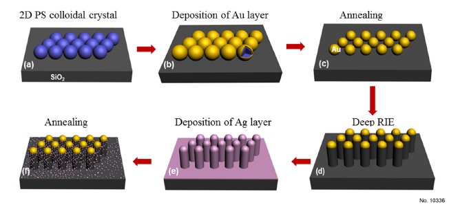
Figure 1: 1. Schematic diagrams of fabrication of the SiO2 nanopillar arrays decorated with Ag NPs. (a)
Monolayer PSs was fabricated on SiO2 wafer by self-assembling process at gas-liquid interface. (b) A
certain thickness of Au film was deposited onto surface of PS spheres by magnetron sputtering
method. (c) After annealing at 1000 C for 2 h to remove the template of PSs, and Au NPs array was
formed. (d) The SiO2 nanopillar arrays were fabricated by deep RIE process. (e) A layer of Ag film
was deposited on the as-formed SiO2 nanopillar arrays by an ion-beam coater with a sputtering
current of 20 mA under different deposition time. (f) After annealing at 600 C for 2 h, SiO2
nanopillar arrays decorated with Ag NPs were formed.
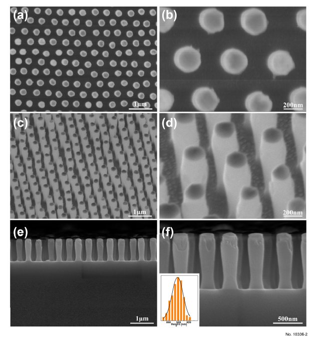
Figure 2: 2. FE-SEM images of periodic SiO2 nanopillar arrays fabricated under etching time of 1500 s:
(a), (c) and (e) is low-magnification image observed from the top, tilted and cross-sectional view,
respectively; (b), (d) and (f) is the corresponding expanded image of (a), (c) and (e) respectively;. The
inset in (f) shows the height distribution of nanopillars in the array.
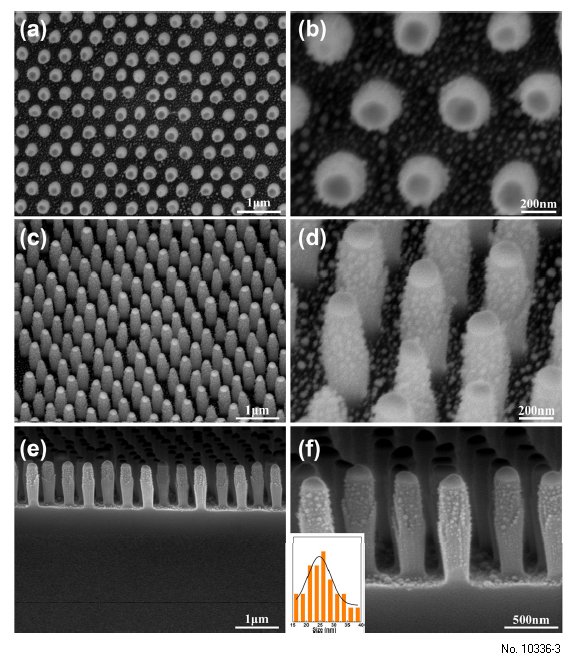
Figure 3: 3. FE-SEM images of periodic SiO2 nanopillar decorated with Ag NPs arrays fabricated under
deposition thickness of Ag layer of 20 nm: (a), (c) and (e) is low-magnification image observed from
the top, tilted and cross-sectional view, respectively; (b), (d) and (f) is the corresponding expanded
images of (a), (b) and (e); The inset in (f) shows the size distribution of Ag NPs on the SiO2
nanopillars.
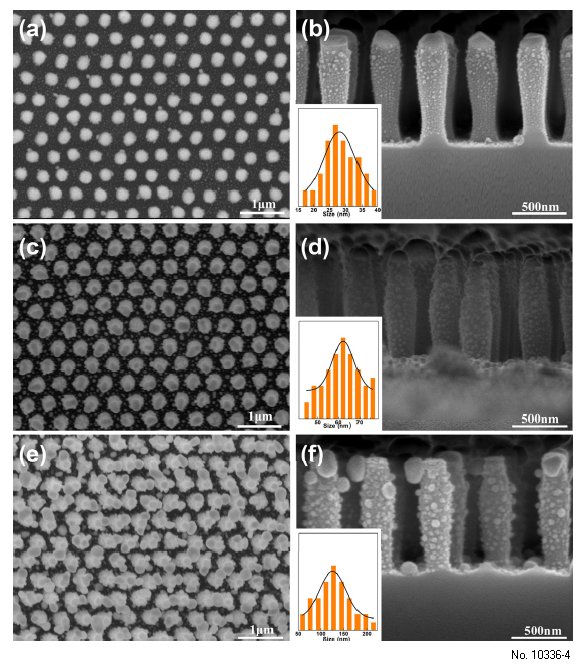
Figure 4: 4. FE-SEM images of periodic SiO2 nanopillar arrays decorated with AgNPs fabricated under
different deposition thickness of Ag layer. (a), (c) and (e) is low-magnification top view image of
deposition thickness of Ag layer of 30 nm, 60 nm and 90 nm, respectively; and (b), (d) and (f) is the
corresponding expanded cross-sectional image of (a), (c) and (e), respectively. The insets in (b), (d)
and (f) show the corresponding size distribution of Ag NPs on the SiO2 nanopillars.