Alphabetical Index
Browse by Elements
Keyword Search
Dry Etchants
Dry and Wet Etchants
Wet Etchants
Bulk Etchants
Layer Etchants
Nano Etchants
Single Crystal Etchants
Thin Film Etchants
Thin Foil Etchants
Wafer Etchants
Al Etchants
Cd Etchants
Ga Etchants
Ge Etchants
In Etchants
New Etchants
Other Etchants
Si Etchants
Zn Etchants
Help
Home
AlN, AlxGa1-xN, and GaN - Wet Etching
Material Name: AlN, AlxGa1-xN, and GaN
Recipe No.: 10344
Primary Chemical Element in Material: Al, Ga
Sample Type: Layer
Uses: Etching
Etchant Name: None
Etching Method: Wet etching
Etchant (Electrolyte) Composition: AlN and GaN bulk substrates were obtained from
HexaTech, Inc. and Kyma, Inc., respectively. GaN bulk crystals
were prepared by hydride vapor phase epitaxy (HVPE)
on sapphire substrates followed by substrate removal. AlN
single crystal wafers were obtained from free standing AlN
single crystalline boules grown by physical vapor transport
(PVT). Detailed information on the substrate properties
and wafer preparation can be found elsewhere. Average
dislocation densities of the AlN and GaN wafers were estimated
to be less than 10 exp(3) cm(2) and 10 exp(6) cm(2), respectively,
based on X-ray topography.
Selective etching of the III-polar and N-polar surface
was obtained using KOH aqueous solution. Etching temperature
was maintained at 70 C, and the concentration of KOH
was approximately 0.18 mol/L. AlGaN bulk crystals are currently
not available. Consequently, investigation of the polarity
etching selectivity of AlN and AlxGa(1-x)N (0 <= x <= 1)
was performed using epitaxial films with thickness around
800 nm grown by metalorganic chemical vapor deposition
(MOCVD) on 2-in. sapphire substrates. Using X-ray diffraction
(XRD), the dislocation density of these films was estimated
to be around 3 x 10 exp(10) cm(2). The investigated films
were fabricated as lateral-polarity-structures (LPS) with
alternating 10 lm wide III-polar and N-polar stripes. An
inertness of III-polar material was established in agreement
with the previous work on GaN and AlN. Consequently, LPS
are ideal structures for KOH etching experiments, since the
change of the height difference between the III-polar and
N-polar stripe is a simple but reliable measure of the etching rate.
The surface morphology of the etched AlN and GaN
bulk crystals was characterized by an Olympus BH-2 differential
interference contrast (DIC) optical microscope.
Scanning electron microscope (SEM) images were recorded
using a JEOL 6400F field emission SEM operating at 5 kV.
TEM cross-section samples were prepared by mechanical
wedge polishing followed by Arþ ion milling (Fischione
Model 1010). TEM imaging was performed with a JEOL
2000FX operated at 200 kV.
Initially, the surface morphology and etch rates of bulk
AlN and GaN crystals were established to allow for comparison
to the AlGaN layers. N-polar surfaces of AlN and GaN
etched under 0.18 mol/L KOH at 70 .C for 60 min are shown
in Figures 1(a) and 1(b), respectively. Both surfaces were
covered with oriented hexagonal etching hillocks with sizes
ranging from 1 µm to 10 µm. In contrast to the N-polar surface,
III-polar GaN and AlN surfaces were nearly inert to KOH wet etching. Ga-polar and Al-polar surfaces remained
atomically smooth after wet etching under the above condition
and no etching pits or hillocks were observed. The etch
rate of both polarities was determined and it was found that
the N-polar surface had an etch rate around 500 nm/min for
AlN and 40 nm/min for GaN, while the etch rates for IIIpolar
AlN and GaN are extremely low. These values yielded
an N-polar AlN to N-polar GaN selectivity higher than 12
and demonstrated the potential of KOH etching for substrate
thinning application or substrate removal from DUV LEDs
grown on AlN single crystalline substrates.
To further investigate the etching selectivity between
AlN and AlGaN, similar wet etching was performed on
AlGaN LPS grown on sapphire substrates. An optical microscope
image of an as-grown Al0.6Ga0.4N LPS (a) and of the
structure after 5 min of KOH etching (b) is shown in Figure
2. The 10 lm wide stripes with alternating III-polar and
N-polar orientation can clearly be distinguished. After the
KOH etching procedure, the III-polar material remained
unchanged. In contrast, the N-polar stripes were significantly
darker, which indicated a significant change of the surface
and thickness of the material.
In order to determine the thickness and etch rate, crosssectional
SEM images of AlxGa(1-x)N LPS before and after
etching were recorded. It was found that the etch rate of the
III-polar AlGaN was below 2 nm/min while the etch rate of
the N-polar surface was significantly higher. This was consistent
with the earlier findings on GaN and AlN. Figure 3
shows SEM images of LPS with two different Al compositions. The red dashed line represents the inversion
domain boundaries. In the as-grown AlN LPS, the N-polar
and III-polar stripes equal in thickness even though the surface
morphology differed (Figure 3(a)). After the sample
was etched in 0.09 mol/L KOH aqueous solution for 6 min,
the N-polar region (~800 nm thick) was completely
removed, exposing the sapphire substrate, see Figure 3(b).
For the sample with 60% Al content, as revealed by Figures
3(c) and 3(d), the height difference between the N-polar and
III-polar Al0.6Ga0.4N changed from 140 nm to 450 nm, which
indicated a decrease in the etch rate with respect to AlN.
The selectivity between the N-polar AlN over N-polar
AlxGa(1-x)N as a function of Al composition is shown in
Figure 4. An etching selectivity to AlN greater than 1 was
observed over the whole compositional range of AlGaN. It
was further observed that the selectivity increased as Al
composition decreased. The maximum etching selectivity of
around 12 was achieved between AlN and GaN LPS. The
etch selectivity obtained under similar conditions for low
dislocation density bulk AlN and GaN crystals was approximately
13. This conforms to the data obtained for the LPS,
although the dislocation density in these structures was several
orders of magnitudes higher than that of the bulk AlN
and GaN materials. This indicated that under these mild
etching conditions, the dislocations did not play a role in the
etching behavior, and this etching scheme was demonstrated to be a very universal substrate removal method for materials
grown by different methods with different crystalline quality.
The formation and development of etching hillocks could
only be attributed to different bonding conditions of crystallographic
planes, which was an intrinsic property of IIInitride
crystal structure.
In order to demonstrate the relationship between etching
hillocks and underlying threading dislocations, thus further
generalize the etching behaviour for various materials’ system,
cross-sectional TEM was performed on N-polar AlN
and GaN after KOH etching at 70 C for 30 min, respectively.
As shown in Figure 5, no dislocations were observed
beneath the hillocks for either of the samples (GaN and AlN)
and either of the diffraction conditions (screw and edge dislocation).
Thus, the etch hillocks could not be associated
with dislocations.
Procedure (Condition): No data
Note: A controllable and smooth potassium hydroxide-based wet etching technique was developed for
the AlGaN system. High selectivity between AlN and AlxGa(1-x)N (up to 12x) was found to be
critical in achieving effective substrate thinning or removal for AlGaN-based deep ultraviolet light
emitting diodes, thus increasing light extraction efficiency. The mechanism of high selectivity of
AlGaN as a function of Al composition can be explained as related to the formation and dissolution
of oxide/hydroxide on top of N-polar surface. Cross-sectional transmission electron microscopic
analysis served as ultimate proof that these hillocks were not related to underlying threading
dislocations.
Reference: W. Guo, R. Kirste, I. Bryan, Z. Bryan, L. Hussey, P. Reddy, J. Tweedie, R. Collazo, and Z. Sitar, KOH based selective wet chemical etching of AlN, AlxGa1-xN, and GaN crystals: A way towards substrate removal in deep ultraviolet-light emitting diode, Applied Physics Letters 106, 082110 (2015); doi: 10.1063/1.4913705.
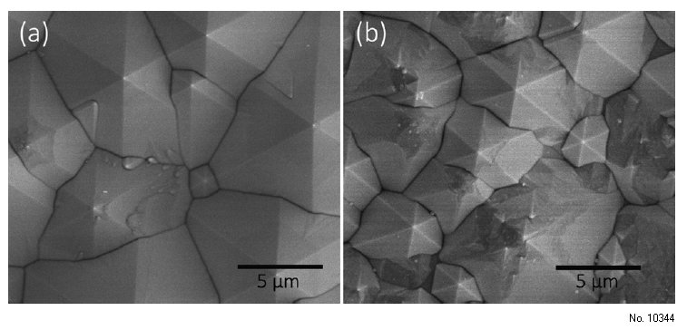
Figure 1: 1. SEM micrographs of N-polar AlN (a) and GaN (b) etched in 0.18
mol/L KOH solutions at 70 C for 60 min.
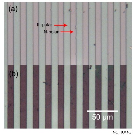
Figure 2: Optical microscope image of an Al0.6Ga0.4N LPS with 10 µm stripes
before (a) and after KOH etching (b).
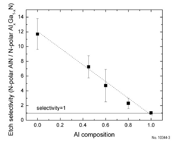
Figure 4: Etch selectivity (AlN/AlxGa1.xN) as a function of Al composition
under KOH (0.09 mol/L, 50 C) etching condition.
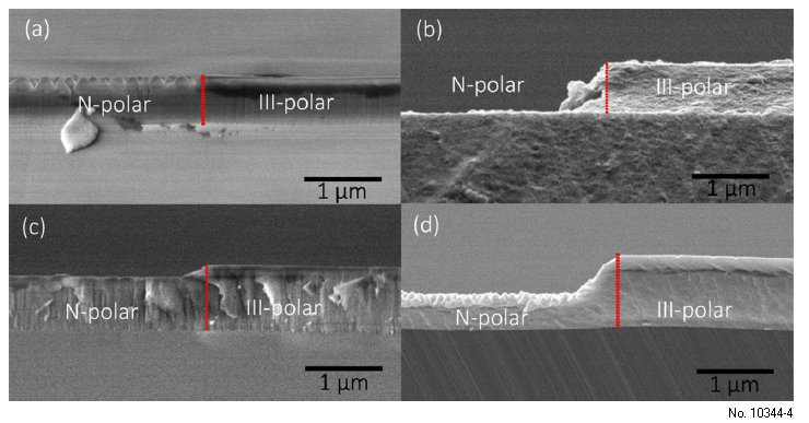
Figure 3: Cross-sectional SEM images
of AlN LPS before (a) and after (b)
etching under 0.09 mol/L KOH solution
at 50 C for 6 min; Al0.6Ga0.4N
LPS before (c) and after (d) etching
under 0.09 mol/L KOH solution at
50 C for 6 min.
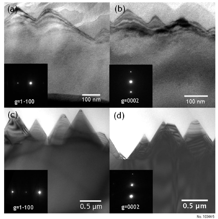
Figure 5: Cross-sectional TEM images
of AlN ((a) and (b)) and GaN ((c) and
(d)) for two diffraction conditions after
KOH etching for 30 min. No correlation
between the hillocks and dislocations
is observed.