Alphabetical Index
Browse by Elements
Keyword Search
Dry Etchants
Dry and Wet Etchants
Wet Etchants
Bulk Etchants
Layer Etchants
Nano Etchants
Single Crystal Etchants
Thin Film Etchants
Thin Foil Etchants
Wafer Etchants
Al Etchants
Cd Etchants
Ga Etchants
Ge Etchants
In Etchants
New Etchants
Other Etchants
Si Etchants
Zn Etchants
Help
Home
Spin-On Carbon (SOC) - Dry Etching
Material Name: Spin-on carbon (SOC)
Recipe No.: 10346
Primary Chemical Element in Material: C
Sample Type: Layer
Uses: Etching
Etchant Name: None
Etching Method: Dry etching
Etchant (Electrolyte) Composition: The polymers tested in this study were synthesized at Brewer Science, Inc. The SOC formulations
were blends of polymers, crosslinkers, catalysts, and other additives. All materials are protected by
patents or are covered in previous technical publications. SOC1 has a low PAB temperature of
225°C. SOC2 has a high hydrogen content and a high PAB temperature of 300°C. SOC3 has a high
hydrogen content and a low PAB temperature of 205°C. These formulations were spin coated on
silicon wafers and baked at the temperatures listed above to cure the films. The multilayer process to
etch into the substrate is shown below in Figure 1.
Lithography Conditions: Each multilayer scheme consisted of one of the three different SOC materials (300 nm) to be tested
for line wiggling, a Si-HM (OptiStack HM9825-302.6 material [26 nm] commercially available
from Brewer Science), and a common commercially available photoresist used in 193-nm
lithography. All these materials were spin coated onto a silicon wafer and baked. After these
materials were applied, they were exposed on an ASML 1250 ArF scanner. Lithography conditions
are listed in Table 1. First a focus-exposure matrix (FEM) wafer was created to find best focus and exposure. Once these
conditions were established, a production-style wafer was produced. Each production-style wafer
was a wafer with one die repeated consistently across the wafer shot at the same dose and focus.
Multilayer-Scheme Pattern Transfer: All pattern transfer experiments were conducted with an Oxford Plasmalab® 80 Plus RIE system
with no end point detection and no inductively coupled plasma (ICP). Step one is the pattern transfer
from photoresist into the Si-HM. See Figure 2.
In this process, the following conditions were used on the etcher: Gas: CF4, Power: 100 watts, Pressure: 50 mTorr.
The etch selectivity of common photoresist to the Si-HM material is about 1:1. Because this is the
first RIE process, the production-style wafers that were exposed by the ASML 1250 were diced up
into chips to enable multiple runs per wafer for experimental use and wafer savings.
The next step in the multilayer RIE process is to transfer the pattern from the Si-HM into the SOC
material. See Figure 3. In this process two different SOC etches were tested on the etcher (Table 2).
The next step in the multilayer RIE process was to transfer the pattern from the SOC material into
the substrate. This process typically is where the SOC will wiggle during the etch, preventing a
successful pattern transfer into the substrate. See Figure 4. In this process, the following conditions were used on the etcher: Gas: C4F4 and Ar mixture, Power: 300 watts ,Pressure: 20 mTorr.
This SOC pattern transfer into the substrate is the process that will determine if we are successful at
eliminating the “wiggle” cased by fluorinated etch processes.
Inspection with SEM Review: The results of RIE in the multilayer scheme were inspected using a LEO 1560 scanning electron
microscope (SEM). The pattern transfer of the photoresist into the Si-HM was achieved for each
SOC material, but this step could not be inspected because cross-sectional SEM analysis is a
destructive inspection and thus would prevent proceeding with SOC transfer into the substrate.
Pattern Transfer of Photoresist into Silicon-Containing Hardmask: Before the material can be tested for wiggling behavior, there first needs to be a systematic process
to evaluate the materials and a control must be established. In this work, the SOC3 material, which is
a dry SOC material with a low PAB temperature of 205°C, consistently wiggled and was used as a
control. Results of the first RIE process of pattern transfer from photoresist to Si-HM is shown
below in Figure 5.
This SEM picture demonstrates successful pattern transfer of the Si-HM material. A slight over-etch
was used in subsequent etch runs because there was no end point detection on the etch tool, all
etches were timed. Therefore, six different times were tested and repeated to ensure the proper
hardmask etch time was established. Also some photoresist remained on top of the Si-HM, but that
would all be removed once the SOC etch begins.
The next step is the pattern transfer of the Si-HM into the SOC materials SOC1 and SOC3. See
Figures 6 and 7.
The cross-sectional SEM images show the successful pattern transfer of the Si-HM into both SOC1
and SOC3. SOC2 was also successfully transferred but is not shown. Each SOC material maintained
it full height of about 300 nm. It should be noted there is still hardmask on top of the SOC material if
further SOC etch is needed. Similar to the hardmask etch, six different etch times were tested and
repeated to find the correct etch time. For Figures 6 and 7, the O2:N2 RIE recipe was used.
Figures 8 and 9 show results for the SOC etch where the RIE recipe used a CO2:Ar gas mixture.
The cross-sectional SEM images make it clear that the gas combination of CO2:Ar was too
aggressive and etched away all the Si-HM material and started to etch into the top of the SOC
material. Due to the need for a higher aspect ratio (line height versus line width), this RIE gas
combination was not used. Similar to previous etches, six etch times were tested and duplicated, and
Figures 8 and 9 show the best results for the process.
Substrate Etch – Wiggle Behavior: Once we had successfully transferred the pattern down through the SOC material, the SOC could be
tested with a fluorinated etch to determine its resistance to wiggling. Also a control must be
established for consistency throughout the experiment. All three SOC materials were tested and retested
on separate days to confirm results. Figure 10 below shows the results for SOC1 at a
fluorinated etch (“wiggle etch”) time of 15 seconds, and Figure 11 shows SOC1 at a fluorinated etch
time of 30 seconds.
Figures 10 and 11 show that SOC1 material did not wiggle after 15 and 30 seconds of wiggle or
substrate etching. Some height loss of about 30 nm occurred, which is expected from the fluorinated
etch. The key result is that the material did not wiggle.
Below are results for the SOC3 material showing the wiggle behavior after only 15 seconds
(Figure 12). Throughout the experiments, the SOC3 material continued to display the wiggle
behavior shown above with only 15 seconds of wiggle etching, therefore making SOC3 a “good”
control for testing.
SOC1 was tested on three different days and gave the same result of no wiggling behavior with an
aspect ratio greater than 5. SOC2 displayed the same wiggle behavior witnessed in the control. In an
effort to increase the aspect ratio to further test SOC1’s resistance to the wiggle etch, the SOC lines
were thinned by over-etching beyond the SOC recipe. This testing was possible because some Si-
HM still remained on top of the lines. Thus, doing a longer etch would decrease the sidewall,
creating a thinner line. The longer SOC etch to thin the lines, and thereby create a larger aspect
ratio, was also performed on the control, SOC3. Figures 14 and 15 show the results of the longer
SOC etch.
In Figure 14 the aspect ratio of the lines standing is ~ 6.25, with a line width of ~ 40 nm and a height
of ~ 250 nm. This proves that SOC1, a material with a low PAB temperature of 225°C, can
withstand the substrate etch successfully and is resistant to wiggling. Also the SOC1 material is spin
bowl compatible and is easily removed with standard developer solution, even after undergoing all
of the SOC RIE.
Procedure (Condition): No data
Note: Spin-on carbon (SOC) materials play an important role in the multilayer lithography scheme for the
mass production of advanced semiconductor devices. One of the SOC’s key roles in the multilayer
process (photoresist, silicon-containing hardmask, SOC) is the reactive ion etch (RIE) for pattern
transfer into the substrate. As aspect ratios of the SOC material increase and feature sizes decrease,
the pattern transfer from SOC to substrate by a fluorine-containing RIE induces severe pattern
deformation (“wiggling”), which ultimately prevents successful pattern transfer into the substrate.
One process that reduces line wiggling is a high-temperature (>250°C) post-application bake of the
SOC material. In this study, we developed a process for evaluating SOC materials with respect to
their pattern transfer performance. This process allowed us to evaluate line-wiggling behavior with
several SOC materials at lower bake temperatures. This paper will discuss novel materials design in
relation to high-aspect-ratio SOC layers and wiggling resistance.
Reference: Michael Weigand, Vandana Krishnamurthy, Yubao Wang, Qin Lin, Douglas Guerrero,
Sean Simmons, Brandy Carr, Evaluating spin-on carbon materials at low temperatures for
high wiggling resistance,
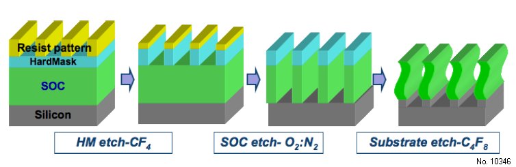
Figure 1: Multilayer scheme process flow.
Table 1: Lithography conditions of ASML 1250 ArF scanner.
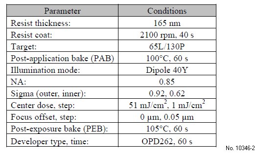
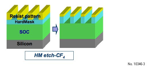
Figure 2: Pattern transfer of photoresist into Si-HM.
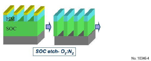
Figure 3: Pattern transfer of Si-HM into SOC material.
Table 2: In this process two different SOC etches were tested on the etcher.
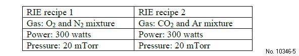
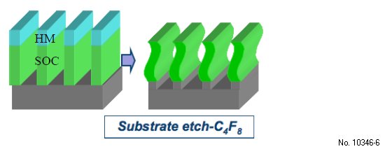
Figure 4: Pattern transfer of SOC material into the substrate.
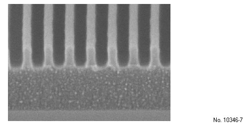
Figure 5: SEM after pattern transfer from photoresist to Si-HM.
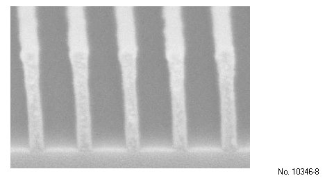
Figure 6: SEM photo taken after pattern transfer from Si-HM into SOC1, O2:N2.
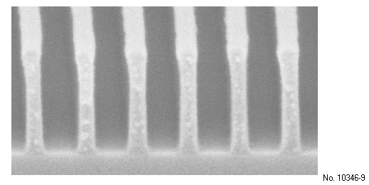
Figure 7: SEM photo taken after pattern transfer from Si-HM into SOC3, O2:N2.
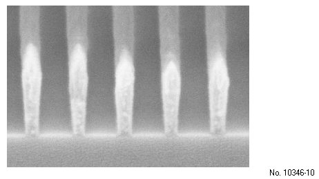
Figure 8: SEM photo taken after pattern transfer from Si-HM into SOC1, CO2:Ar
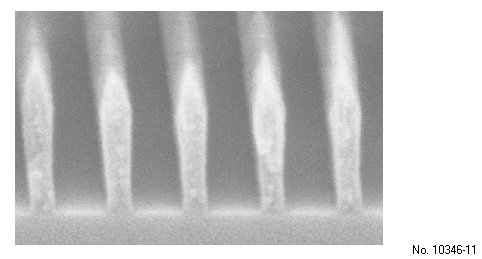
Figure 9: SEM photo taken after pattern transfer from Si-HM into SOC3, CO2:Ar
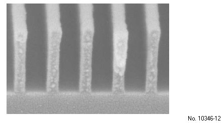
Figure 10: SEM photo of SOC1 taken after 15-second wiggle etch.
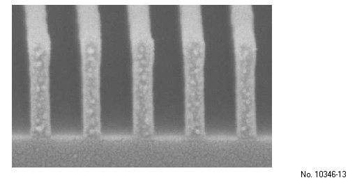
Figure 11: SEM photo of SOC1 taken after 30-second wiggle etch.
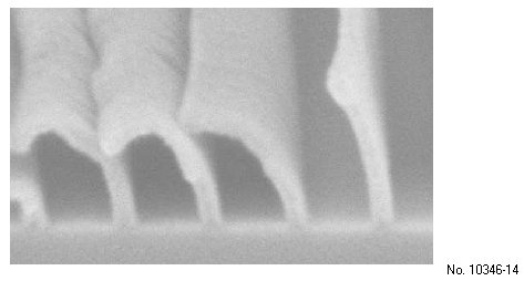
Figure 12: SEM photo of SOC3 taken after 15-second wiggle etch.
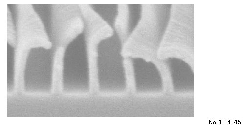
Figure 12: SEM photo of SOC3, control, taken after 15-second wiggle etch.
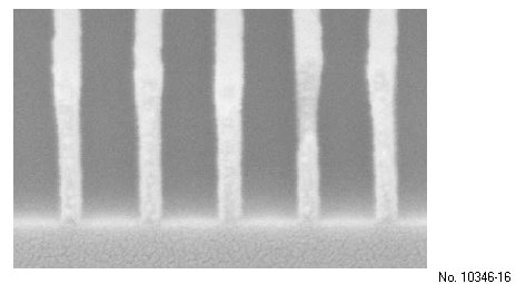
Figure 13: SEM photo of SOC1, aspect ratio: ~ 6.25.
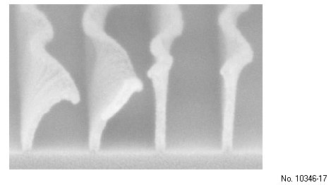
Figure 14: SEM photo of SOC3, control.