Alphabetical Index
Browse by Elements
Keyword Search
Dry Etchants
Dry and Wet Etchants
Wet Etchants
Bulk Etchants
Layer Etchants
Nano Etchants
Single Crystal Etchants
Thin Film Etchants
Thin Foil Etchants
Wafer Etchants
Al Etchants
Cd Etchants
Ga Etchants
Ge Etchants
In Etchants
New Etchants
Other Etchants
Si Etchants
Zn Etchants
Help
Home
InAs/GaSb - Wet Etching
Material Name: InAs/GaSb
Recipe No.: 10347
Primary Chemical Element in Material: In, Ga
Sample Type: Layer
Uses: Etching
Etchant Name: None
Etching Method: Wet etching
Etchant (Electrolyte) Composition: This study focuses on the sidewall roughness
and crystallographic orientation selectivity of
mid-wave and long-wave InAs/GaSb SL photodiodes
while wet etching with etchants based on
H3PO4/H2O2/H2O/C6H8O7. The etching of InAs
and GaSb bulk materials is also examined in this work.
After photolithography of the MWIR and
LWIR materials, a chemical solution based on
H3PO4/H2O2/H2O/C6H8O7 was used for wet etching,
where the phosphoric acid (85%), hydrogen peroxide
(30%) and citric acid (100.0%) solutions were
mixed in different proportions. Prior to wet etching,
the samples were cleaned by acetone, absolute ethyl
alcohol and deionized water to remove organic impurities,
with a subsequent cleaning in hydrochloric acid
(3.5%) to remove the surface oxides. The samples were
then rinsed in deionized water and dried with N2 gas.
The etching rates varied for the different solutions,
and the sidewall angles and roughness also varied.
To understand the mechanisms of InAs/GaSb SLs
wet mesa etching, the InAs and GaSb materials were
etched separately by using H3PO4/H2O2/H2O and
H3PO4/H2O2/H2O/C6H8O7 solutions in varying proportions
for InAs and GaSb substrates, respectively.
To analyze the process of chemically etching InAs/GaSb SL photodiodes under various conditions,
we vary the proportions of the four wet chemical
etchant components including H3PO4, H2O2, C6H8O7
and H2O, and observe the roughness of the mesa sidewalls
and the etch depth (i.e., etching rates) via scanning
electron microscopy (SEM). The sidewall roughness
can be observed via the SEM images, while they
cannot be used to measure the roughness. However,
the sidewall roughness can be inferred from the surface
roughness after etching, and the results of data
from atomic force microscopy (AFM) and the SEM
images also verify this relationship.
Firstly, we focus on the MWIR and study the role
of hydrogen peroxide in the etchant, where the etching
rates and the surface roughness are given in Table
2 and in Fig. 1(a). It can be seen that, when the hydrogen
peroxide reaches a threshold value, it cannot
influence the etching rate. Instead, after the hydrogen
peroxide reaches its threshold value, the sidewall
roughness increases with the proportions of hydrogen
peroxide. Figure 1(b) shows an AFM image of the
surface exhibiting the greatest and least amount of
roughness.
Next, the roles of citric acid and phosphoric acid in
etching the MWIR are studied, and the etching rates
and sidewall images are given in Tables 3 and 4. It
can be seen that the final etching rate is more correlated
with the phosphoric acid and that increased
smoothing of the sidewalls and surface occurs with
increasing the proportions of citric acid. The corresponding
experiments examining the variation of the etchant components on the LWIR InAs/GaSb SLs exhibit
the same variational tendency in the etching
rates and roughness values as those seen in the MWIR
InAs/GaSb SLs.
The presence of complex MPO4 (i.e., InPO4,
GaPO4, AsPO4 and SbPO4) and oxides on the surface,
however, can strongly deteriorate the mesa surface
sidewalls, thus citric acid is used to increase
the smoothness of the sidewalls. After the experiment,
we obtain an optimized chemical solution
(C6H8O7:H3PO4:H2O2:H2O=0.75 g:1 ml:0.6 ml:2 ml)
for MWIR InAs/GaSb SLs with an etching rate of 200 nm/min, which produces much smoother sidewalls
than the previous etchant (citric acid solution
:H3PO4 :H2O2 :H2O=1ml : 1ml : 2 ml : 20 ml, citric
acid solution=C6H8O7 :H2O=1g : 1 ml).
In addition, the results of the InAs and GaSb materials
show that InAs etchants without citric acid also
produce sidewalls with excellent performances, and
the GaSb etching requires a more highly concentrated
solution than that previously used for InAs/GaSb SLs.
Therefore, if we increase the amount of InAs in the
SLs, we can reduce the amount of citric acid and, likewise,
if the amount of GaSb is increased, an etchant
with a higher concentration is needed.
There is an obvious anisotropy seen in the etching
profile of InAs materials, and in an attempt to
reduce this anisotropy we tried different (100) substrates
and etchants based upon H3PO4/H2O2/H2O,
shown in the SEM image in Fig. 3(a). Although the
angles and turning positions vary, the etching profiles
are all in the same situation as that shown in Fig. 3(b).
We now compare the four different kinds of materials
including InAs, GaSb, MWIR SLs and LWIR
SLs, whose profiles are shown in Fig. 4, where it can be seen that, even in the same crystallographic orientation,
wet chemical etching of InAs and GaSb has
markedly different profiles. From the SEM profiles of
the MWIR and LWIR SLs, we can see that the profile
of each InAs/GaSb SLs corresponds to that of its
most prevalent component. For example, LWIR SLs
with more InAs have the profile most similar to that
of InAs bulk materials.
Procedure (Condition): No data
Note: The roughness and the crystallographic orientation selectivity of etched antimonide-based infrared materials are
examined and are used to optimize the chemical mesa etching process of the InAs/GaSb superlattice photodiode
with the goal of reducing the dark current. The etchant used is based on phosphoric acid (H3PO4), citric acid
(C6H8O7) and hydrogen peroxide (H2O2). The roughness of the mesa sidewalls and etching rates are compared
and used to find an optimized etchant.
Reference: HAO Hong-Yue, et al., Wet Chemical Etching of Antimonide-Based Infrared Materials, CHIN. PHYS. LETT. Vol. 32, No. 10 (2015) pp. 107302-1 - 107302-4.
Table 1: The structures of MWIR and LWIR InAs/GaSb photodiodes.
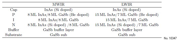
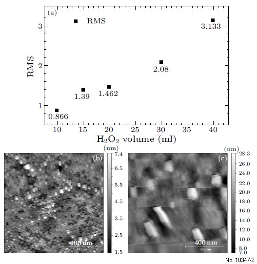
Figure 1: (a) Surface roughness materials in different
etchants. (b) AFM image of the surface.
Table 2: Etching rate with different volumes of hydrogen peroxide.
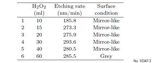
Table 3: Etching rate and surface roughness with increasing
the citric acid.
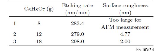
Table 4: Etching rate in etchants with different phosphoric
acids.
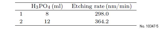
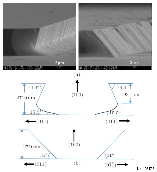
Figure 3: Nonisotropic of InAs wet etching shown by (a)
SEM images and (b) plots.
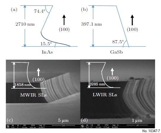
Figure 4: Profiles of (a) InAs, (b) GaSb, (c) MWIR SLs and
(d) LWIR SLs in the (011) crystallographic orientation.