Alphabetical Index
Browse by Elements
Keyword Search
Dry Etchants
Dry and Wet Etchants
Wet Etchants
Bulk Etchants
Layer Etchants
Nano Etchants
Single Crystal Etchants
Thin Film Etchants
Thin Foil Etchants
Wafer Etchants
Al Etchants
Cd Etchants
Ga Etchants
Ge Etchants
In Etchants
New Etchants
Other Etchants
Si Etchants
Zn Etchants
Help
Home
Si, Ge, and Ge:P - Dry Etching
Material Name: Si, Ge, and Ge:P
Recipe No.: 10354
Primary Chemical Element in Material: Si, Ge
Sample Type: Wafer
Uses: Etching
Etchant Name: None
Etching Method: Dry etching
Etchant (Electrolyte) Composition: In this experiment, 100mm diameter, low-doped (1–10 Ohm x cm) Si(001) substrates were used and Ge and Ge:P layers
grown on the Si substrates. Growth was performed by
reduced pressure chemical vapor deposition in an ASM
Epsilon 2000 reactor using germane (GeH4), where the specific
growth properties and material properties of these
layers have been previously reported.1 The doping concentrations
of the final Ge layer were 1 x 10 exp(18) cm(-3) (herein
referred to as “lightly doped,” Ge:P[L]) and a 3 x 10 exp(19) cm(-3)
(referred to as “heavily doped,” Ge:P[H], respectively.
a) Schematic diagrams of the samples are presented in Fig. 1.
The investigation was performed on small (7 x 7 mm2)
pieces of the grown wafer where photolithography was performed
using a 1.8 µm S1813 photoresist, a Karl Suss MJB4
mask aligner, and MF-319 developer to create mesas of photoresist
of width 8 µm, and 8 µm spacing, and 2mm long,
alighted along the <1 1 0> direction. Samples were cleaned
by deionized water and then dried with nitrogen.
The apparatus for dry etching used in this work was the
Corial 200 IL operating at a frequency of 13.6 MHz and using
gas sources of SF6 (99.999%), O2 (99.9995%), and He
(99.999%) as a temperature control gas to a handle wafer,
upon which the sample was placed. All fabrication equipment
used was housed and operated in a class 100 clean room. The
RIE process parameters were: working pressure of 20 mTorr,
RF power 100 W, and total gas flow of 30 sccm. A cooling system was used to keep the handle wafer at a constant temperature
of 20 C throughout the etch process. Surface steps were measured using an Ambios XP-100
step-profilometer. After RIE, the mesa height was measured
postresist removal, an example of which is shown in Fig. 2.
The mesa step without resist measured the vertical amount
of material removed and in conjunction with the etch time
this determining the etch rate. To investigate the results of
anisotropy, samples were then cleaved along h1 1 0i directions
across the mesas so that their cross-sections could be
examined by secondary electron microscopy (SEM) using an
accelerating voltage of 5 kV and a Zeiss Supra InLens backscattered
electron detector.
Figure 3 shows the measured etch rates versus O2 dilution
(%O2). A sharp rise in etch rate is observed for all samples
when O2 was introduced into the SF6 up to% O2 of 5%, and
then fell as the O2 dilution was increased beyond this value.
Specifically, the Si etch rate declines linearly as %O2
increases from 5% to 50%, and then has a slow linear reduction
up to 90%. Ge and Ge:P etch rates rapidly decline as %O2 increases to 20%, above which the etch rate levels off
and remains roughly constant up to 70%O2, approaching
zero at 90%. The effect of doping level upon the etch rate is
more significant at lower O2%, where the etch rate of the
lighter doped Ge:P[L] is higher than the intrinsic Ge (i-Ge),
which are both higher than that of heavily doped Ge:P[H].
Where O2>20%, the etch rate of all types of Ge samples
are similar and does not show any differences. Overall, the
O2 content has a larger influence on etch rate compared to
doping level when O2 content is more than 20%, whereas
doping effects are more prevalent with O2 content below 20%.
Sidewall profile
Our definition for the etch sidewall profile and the associated
measured angle11 are shown in Fig. 4. The samples are
patterned on the h110i directions and are cleaved using
standard cleaving techniques perpendicular to the mesa
direction. The etched mesas are analyzed by SEM and anisotropic
etching is evident for all samples, where images of the
sidewalls are shown in Fig. 5 and are presented graphically
in Fig. 6. When the Si and Ge sidewall angles are compared,
it is observed that there is no significant difference. The perfect
anisotropic mesa, where theta=90 deg., is achieved with
%O2¼20%. This is the critical concentration beyond which
the angle changes from acute to obtuse; these observations
are consistent with a transition between plasma-to-sputter--
dominated etching, the isotropic profile being caused by
plasma etching and anisotropic profile through physical
etchting.
Reactive ion etching of Si, Ge, and Ge:P has been studied,
using an SF6-O2 gas mixture. The etch rate rises sharply as
small amounts of O2 (up to 5%) are added to a pure SF6 etch
and then decreases when the O2 content is increased further.
The etch rate of Ge and Ge:P is significantly increased over
Si for O2 content in the ranges 0% to 12% and >46%, indicating
that well-controlled selective etching is achievable
simply by varying O2 flow rates. Perfectly perpendicular
sidewalls are also clearly evident close to 20% O2 content,
again allowing excellent etching control. Future work could
usefully investigate the depth of trenches with vertical sidewalls
that could be made using this processing condition. In
summary, adding O2 to SF6 for RIE applications enables significant
advantageous and well controllable variations in the process.
Procedure (Condition): No data
Note: The impact of the O2 content in SF6-O2 gas mixtures on the etch rate and sidewall profile of silicon
(Si), germanium (Ge), and phosphorous doped germanium (Ge:P) in reactive ion etching has been
studied. The characteristics of etch rate and sidewall profile are greatly affected by the O2 content.
Below 50% of O2 content, a large variation in Ge etch rates is found compared to that of Si, but for
O2 content above 50% the etch rates follow relatively the same trend. Lightly doped Ge shows the
highest etch rate at a O2 concentration up to 20%. Sidewall angles range from a minimum of 80. to
a maximum of 166., with O2 concentration of 20% yielding perfect anisotropic mesa etch. Also at
this O2 concentration, reasonable Si/Ge selectivity is possible. These observations indicate that by
adjusting the O2 concentration, precision plasma etching of Si, Ge, and Ge:P is possible.
Reference: Wongwanitwattana, Chalermwat, Shah, Vishal Ajit, Myronov, Maksym, Parker, Evan H.
C., Whall, Terry E. and Leadley, David R.. (2014) Precision plasma etching of Si, Ge,
and Ge:P by SF6 with added O2. Journal of Vacuum Science & Technology A: Vacuum,
Surfaces, and Films, Volume 32 (Number 3). Article number 031302. ISSN 0734-2101.
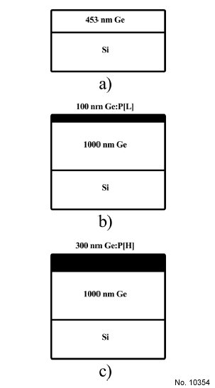
Figure 1: Schematics of samples: (a) Ge (undoped layer); (b) Ge:P[L] (1 x 10 exp(18) cm(-3); and (c) Ge:P[H] (3 x 10 exp(19) cm(-3).
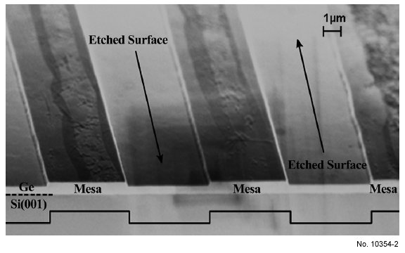
Figure 2: Ge mesa pattern using RIE, removed photoresist (PR) (still have residual PR).
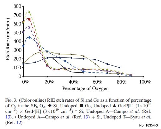
Figure 3: (Color online) RIE etch rates of Si and Ge as a function of percentage
of O2 in the SF6-O2.
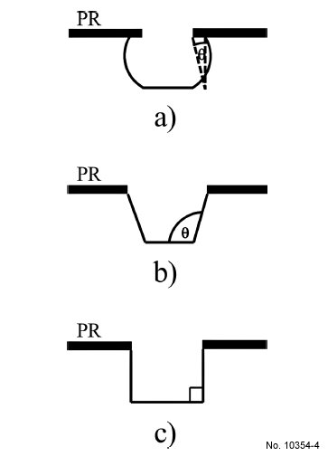
Figure 4: Mesa profiles produced by anisotropic and isotropic etching
(PR= photoresist): (a) Isotropic, (b) partially anisotropic, and (c) perfect
anisotropy.
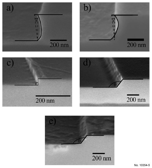
Figure 5: SEM images of the surface morphology of Ge mesa after dry etching
with SF2-O2 of various O2 percentages: (a) 0%, (b) 5%, (c) 20%, (d) 50%,
and (e) 70%.
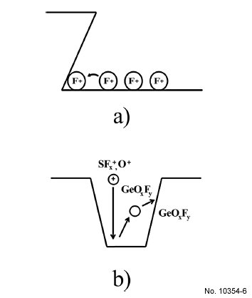
Figure 7: Proposed etch mechanism: (a) the Fþ ions find the site of least potential
energy, the step and therefore etch slightly laterally. (b) GeOxFy is sputtered
from the bottom surface and redeposited onto the sidewall.