Alphabetical Index
Browse by Elements
Keyword Search
Dry Etchants
Dry and Wet Etchants
Wet Etchants
Bulk Etchants
Layer Etchants
Nano Etchants
Single Crystal Etchants
Thin Film Etchants
Thin Foil Etchants
Wafer Etchants
Al Etchants
Cd Etchants
Ga Etchants
Ge Etchants
In Etchants
New Etchants
Other Etchants
Si Etchants
Zn Etchants
Help
Home
CoSi2/Si - Wet Etching
Material Name: CoSi2/Si
Recipe No.: 10357
Primary Chemical Element in Material: No data
Sample Type: Thin film
Uses: Etching
Etchant Name: None
Etching Method: Wet etching
Etchant (Electrolyte) Composition: Cobalt nitride films on Si and SOI substrates were prepared
by CVD using bis(N-tert-butyl-Nüf-ethyl-propionamidinato) cobalt(II)
and a mixture of 20 sccm NH3 and 40 sccm H2 at 200 C. The details
of this process have been described elsewhere. The Si and SOI substrates
were first treated by UV-ozone and then cleaned by HF before
deposition. After cleaning, the substrates were immediately placed
into the reactor chamber and evacuated, to suppress oxidation of the
substrates. As Co is unable to react with SiO2, the cobalt silicide
formation might be slowed down or even blocked by any interfacial
native oxide. Therefore, a clean substrate without native oxide is
critical to obtain a uniform and smooth CoSi2 films.
The as-deposited CoxN films were treated by in-situ RTA at elevated
temperatures from 500 C to 700 C for 30 sec in purified N2.
Those gases used in the deposition and annealing processes were purified
by gas purifiers (Entegris Gatekeeper) to reduce the impurities below
1 ppb for all contaminants including O2, CO,CO2, and H2O. This
purification is needed because the CoSi2 formation process is highly
sensitive to traces of oxygen-containing impurities in the annealing
ambient. Extremely low levels of these impurities are essential for
smooth CoSi2 formation. Indeed, attempts to form CoSi2 from CoxN
by ex-situ RTA were unsuccessful owing to the sample contamination
during the exposure to the air and the annealing ambient (our ex-situ
RTA tool does not use purified gas for annealing). Those impurities
resulted in discontinuous CoSi2 with many voids. A previous study
also showed that impurities in the annealing atmosphere formed voids
during silicidation. Therefore, we employed in-situ annealing inside
our cobalt deposition system to produce consistent, continuous CoSi2 films.
The back side sample preparation included 5 steps to reveal the
CoSi2/Si interface. First, the sample was bonded upside down to a
glass slide of similar size for mechanical support. Epoxy Bond 110
(Ted Pella Inc.) is used for bonding the two. Thin epoxy glue was
carefully applied in between and degassed, then cured at 125 C for
10 min to obtain a homogenous glue film with good adhesion.
Second, the bonded sample stack was mounted onto a specimen
mount - a cylindrical Pyrex stub (Gatan Inc.) using a low-meltingpoint
wax (Crystalbond 509, Ted Pella Inc.). The stub was heated on a
hot plate at 130 CŁ160 C to melt a tiny granule of wax for mounting
the sample stack to be ground flat. Then a metal ring (Gatan Inc.)
was used to hold the stub flat on the polishing sand paper. Rough
thinning of the specimen was performed with a polisher (Allied High
Tech Products Inc.) until a thickness of 100 µm or less was achieved.
The thickness of the specimen was measured and monitored by the
micrometer to reach the desired thickness of less than 100 µm after
polishing. The Si substrate was coarsely polished sequentially by SiC sand paper of 600 grit and 1200 grit. The polished specimen was
detached from the mounting stub by melting the wax on a hot plate
and dissolving the remaining wax in acetone.
Third, the remaining Si substrate was removed by a heated TMAH
(25 wt%) bath at 85 C. TMAH etching is highly selective toward
the thermal oxide. Thus when no more bubbles were formed in the
etching solution, it indicated the bulk Si had been completely removed,
exposing the SiO2 layer. Then the sample was immersed in 10:1
buffered HF solution until the SiO2 layer of the SOI was removed,
which is the fourth step.
In the final step, the remaining Si layer (~100 nm) from SOI
(originally 200 nm) was removed by dry etching with XeF2 gas.
This was performed in a home-built XeF2 etching tool. Exposed Si
was quickly etched by alternating exposure to XeF2 and subsequent
pumping away of gaseous reaction products. Si reacts with XeF2 to
form gaseous Xe and SiF4. XeF2 etching has been used to selectively
remove Si because it removes only silicon, but not photoresist, SiO2,
silicon nitride, Al, Cr, or TiN. We measured that in our system the
XeF2 etch rate of CoSi2 is 200 times slower than that of Si; thus XeF2
etching can selectively remove the thin layer of residual Si. As a result
of the excellent selectivity toward CoSi2, the XeF2 etching process is
highly robust and tolerant toward some over-etch. This final step leaves
a clean CoSi2 surface, allowing the CoSi2/Si interface to be examined
by atomic force microscopy (AFM). The interfacial roughness study
is valuable for optimizing cobalt silicide process.
Procedure (Condition): No data
Note: The formation of smooth, conformal cobalt disilicide (CoSi2) without facets or voids is critical for microelectronic device reliability
owing to the ultra-shallow contact areas. Here we demonstrate the formation of smooth and conformal CoSi2 films by chemical
vapor deposition (CVD) of cobalt nitride (CoxN) films on silicon (Si) or on silicon on insulator (SOI) substrates, followed by in-situ
rapid thermal annealing (RTA) at 700 C. To reveal the CoSi2/Si interfacial morphology, we report a back-to-front sample preparation
method, in which mechanical polishing, anisotropic tetramethylammonium hydroxide (TMAH) wet etching, hydrofluoric acid (HF)
wet etching, and isotropic xenon difluoride (XeF2) dry etching are employed to remove the SOI substrate from the back side to expose
the CoSi2/Si interface. This method offers a robust and reliable procedure for quantitative assessment of the CoSi2/Si interfacial
roughness, as well as analytical support for advanced fabrication process development.
Reference: Jing Yang, et al., Quantitative Evaluation of Cobalt Disilicide/Si Interfacial
Roughness, ECS Journal of Solid State Science and Technology, 6 (5) P345-P349 (2017).
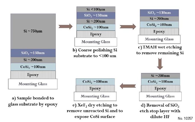
Figure 1: Schematic representation of consecutive steps in back side sample preparation procedure to reveal CoSi2/Si interface: Sample is prepared by annealing
CoxN on SOI substrate at 700 C to form CoSi2 on SOI. (a) Sample is invert and fixed on a support glass substrate of approximately same size. (b) Sample after
grinding the back side substrate with SiC sand paper (600 - 1200 grit) to reduce substrate thickness down to below 100 µm. (c) Sample after TMAH wet etching
to selectively remove the residual silicon substrate. (d) Sample after a dilute HF etching to remove the exposed buried oxide. (e) Sample after dry XeF2 etching to
selectively remove the residual unreacted silicon, leaving the CoSi2 surface ready for AFM measurements.