Alphabetical Index
Browse by Elements
Keyword Search
Dry Etchants
Dry and Wet Etchants
Wet Etchants
Bulk Etchants
Layer Etchants
Nano Etchants
Single Crystal Etchants
Thin Film Etchants
Thin Foil Etchants
Wafer Etchants
Al Etchants
Cd Etchants
Ga Etchants
Ge Etchants
In Etchants
New Etchants
Other Etchants
Si Etchants
Zn Etchants
Help
Home
ZnO:Al Thin Film - Wet Etching
Material Name: ZnO:Al
Recipe No.: 10360
Primary Chemical Element in Material: Zn
Sample Type: Thin film
Uses: Etching
Etchant Name: None
Etching Method: Dry etching
Etchant (Electrolyte) Composition: ZnO:Al films were reactively sputtered on glass substrates (Corning, Eagle XG) in a vertical
in-line sputtering system (VISS 300, by von Ardenne Anlagentechnik, Dresden, Germany). The
system is typically under a base pressure of 6×10 exp(-4) Pa. Rotatable dual magnetron cathodes (RDM)
with metallic Zn:Al tube targets (0.5 wt%) were operated at discharge power of 10 kW with
mid-frequency excitation of 40 kHz to achieve a growth rate of up to 90 nm·m/min. The process
pressure, Argon gas flow and substrate temperature were respectively 0.96 Pa, 200 sccm and
350°C as measured via heat radiation prior to deposition. The working point was controlled via
plasma emission monitor (PEM) in the transition mode at PEM intensity of 35 % and average
oxygen gas flow of 160 sccm. More details on PEM control can be found in literature. A
related paper provides more detailed information on ZnO:Al film properties. As-grown
ZnO:Al films with low resistivity of less than 4×10⁻⁴ O·cm were used for etching experiments
followed in this study. ZnO:Al films were etched in aqueous solutions of diluted hydrofluoric (HF
1%) or hydrochloric (HCl 0.5%). As reference material we used a ZnO:Al film sputtered at low
rate from ceramic tube targets in the same deposition system, as such ZnO:Al films could achieve
excellent light trapping upon HCl etching in silicon based thin film solar cells.
The thicknesses were measured with surface profiler. The electrical properties of the films
were investigated by 4-point probe and Hall effect measurement using van der Pauw method. The
morphologies of as-deposited and etched ZnO:Al films were evaluated by atomic force
microscopy (AFM, Nanoscope system from Veeco). Optical transmission and reflection of surface
textured thin films were carried out with a double beam spectrometer equipped with an integrating
sphere (Perkin Elmer Lambda). An index matching fluid (CH2I2) was used to avoid systematic measurement errors due to light scattering of the rough films during optical measurement for
absorption determination.
We studied the ZnO:Al film properties after etching. Fig.1 shows the variation of thickness
and sheet resistance as well as root mean square (RMS) roughness of ZnO:Al films after two-step
etching first in HF (120 sec) and then in HCl. The values given at negative times correspond to the
as-grown ZnO:Al film. The etch times correspond to the second etch step in 0.5 % HCl. Thickness
(solid square) first decreases by about 150 nm by etching in HF solution for 120 s, and then
decreases gradually from 720 nm to 550 nm with the increase of etching time in HCl solution.
Sheet resistance (solid circle) increases with the decrease of thickness from about 3.8 Omega to 9 Omega.
RMS roughness (solid triangle) rises from about 10 nm to about 90 nm by the first etching step.
During the second etching step the RMS roughness shows a maximum of about 100 nm at 8 s and
then decreases again for long etch times. In addition, the data of ZnO:Al film is shown, that was
etched only by a single etching in HCl solution for 60 s. The sheet resistance is about 4.5 Omega due to
its relatively high thickness (800 nm). The depth of large craters of these films is about 200 nm.
Even though the films are etched for long time in HCl solution, the RMS roughness cannot be
raised above 60 nm. Upon a longer etching time the films would suffer from holes that are etched
to the glass.
Procedure (Condition): No data
Note: Highly transparent and conductive aluminum doped zinc oxide thin films (ZnO:Al) were
reactively sputtered from metallic targets at high rate of up to 90 nm·m/min. For the application as
transparent light scattering front contact in silicon thin film solar cells, a texture etching process is
applied. Typically, it is difficult to achieve appropriate etch features in hydrochloric acid, as the
deposition process must be tuned and the interrelation is not well understood. We introduce a
novel two step etching method based on hydrofluoric acid. By tuning the etch parameters we
varied the surface morphology and achieved a regular distribution of large craters with the feature
size of 1-2 µm in diameter and about 250 nm in depth. Microcrystalline silicon single junction
solar cells (µc-Si:H) and amorphous/microcrystalline (a-Si:H/µc-Si:H) tandem solar cells with
high efficiency of up to 8.2% and 11.4%, respectively, were achieved with optimized ZnO:Al
films as light scattering transparent front contact.
Reference: H. Zhu, et al., Novel etching method on high rate ZnO:Al thin films reactively
sputtered from dual tube metallic targets for silicon based solar cells, Solar Energy Materials & Solar Cells 95 (2011) 964 - 968.
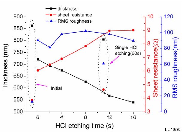
Figure 1: Variations of thickness and sheet resistance as well as RMS roughness of high growth rate
ZnO:Al films upon etching: Negative etch times correspond to initial values before etching, the
values at 60 s correspond to single step etching in HCl; all other values correspond to the second
HCl step after a first HF etch.