Alphabetical Index
Browse by Elements
Keyword Search
Dry Etchants
Dry and Wet Etchants
Wet Etchants
Bulk Etchants
Layer Etchants
Nano Etchants
Single Crystal Etchants
Thin Film Etchants
Thin Foil Etchants
Wafer Etchants
Al Etchants
Cd Etchants
Ga Etchants
Ge Etchants
In Etchants
New Etchants
Other Etchants
Si Etchants
Zn Etchants
Help
Home
Chalcogenide Glasses (ChG)-Ge23Sb7S70 - Dry Etching
Material Name: Chalcogenide glasses (ChG)-Ge23Sb7S70
Recipe No.: 8515
Primary Chemical Element in Material: Ge
Sample Type: Thin film
Uses: Etching
Etchant Name: None
Etching Method: Dry etching
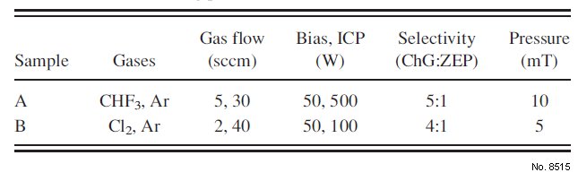
Etchant (Electrolyte) Composition: Plasma etching was performed using a Unaxis
Shuttleline inductively coupled plasma reactive ion etcher
(ICP-RIE). Two different etching recipes based on CHF3 and
Cl2 were investigated in order to determine the best performance
(see Table 1). Both samples A and B were etched by
approximately 290 nm at a temperature of 20 C. Sample A
had a thickness of 600 nm, and sample B was 650 nm thick.
After etching, the samples were coated with a benzocyclobutene
(BCB) polymer cladding to protect the surfaces from
contamination and to reduce scattering from the sidewalls.
The curing of the polymer was performed in a nitrogen oven
at a maximum temperature of 220 C.
Procedure (Condition): Fabrication started with standard solvent cleaning of
100-mm diameter silicon wafers with 2 µm of thermal oxide
grown on the surface. Electron-beam deposition was used to
produce the ChG films on the surface of the silicon dioxide.
This deposition method has been previously reported,11 and
is further investigated here under different deposition conditions.
The deposition was performed at a rate of about 1 nm/a) s, starting with 1.1 cm2 cylindrical rods of bulk glass with the composition Ge23Sb7S70. Bulk Ge23Sb7S70 glass was fabricated
by traditional melt quenching techniques A film approximately 630-nm-thick was deposited on the surface of the wafer.
Note: No data
Reference: Jeff Chiles, et al., Low-loss, submicron chalcogenide integrated photonics with chlorine
plasma etching, APPLIED PHYSICS LETTERS 106, (2015), pp. 111110-1 - 111110-4.
Table 1: Plasma etching parameters.