Alphabetical Index
Browse by Elements
Keyword Search
Dry Etchants
Dry and Wet Etchants
Wet Etchants
Bulk Etchants
Layer Etchants
Nano Etchants
Single Crystal Etchants
Thin Film Etchants
Thin Foil Etchants
Wafer Etchants
Al Etchants
Cd Etchants
Ga Etchants
Ge Etchants
In Etchants
New Etchants
Other Etchants
Si Etchants
Zn Etchants
Help
Home
Sub Surface Cu Voids
Material Name: Copper
Record No.: 110
Primary Chemical Element in Material: Cu
Sample Type: Layer
Uses: Etching
Etchant Name: None
Etching Method: Dry etching
Etchant (Electrolyte) Composition: No data
Procedure (Condition): No data
Note: Copper voiding is major headache in the megafab
production of IC's. Copper can form as many as four
different types of voids, necessitating constant vigilance and tight process
control. FIB sectioning of void test structures is a destructive
but effective method to monitor process induced
voids. See Figures (14-16) below. Sub surface Cu voiding is particularly hard to detect
because it neither visible to "top view" KLA-like
inspections and rarely results in a full electrical
opens. Thus slower and destructive techniques are
required to monitor the process. Passive FIB voltage
contrast is especially helpful with well-designed test
structures.
Reference: Bryan Tracy, Materials Analysis and Process Monitoring in MegaFabs, ISTFA 2002, Proceedings of the 28th International Symposium for Testing and Failure Analysis, 3-7 November 2002, Phoenix Civic Center, Phoenix, Arizona, pp. 69-75.
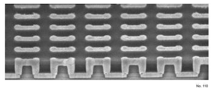
Figure 1: SEM of a M2/M1 via void test structure.
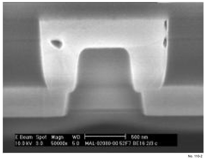
Figure 2: Bulk and via sidewall voids.
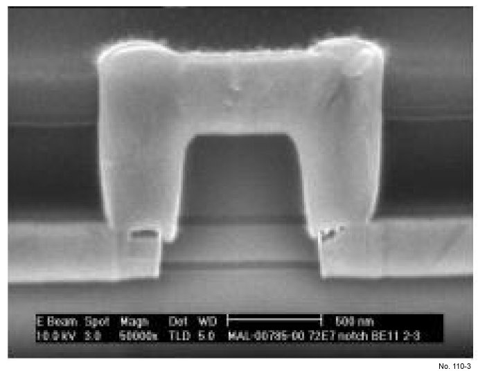
Figure 3: Cap interface voids.