Alphabetical Index
Browse by Elements
Keyword Search
Dry Etchants
Dry and Wet Etchants
Wet Etchants
Bulk Etchants
Layer Etchants
Nano Etchants
Single Crystal Etchants
Thin Film Etchants
Thin Foil Etchants
Wafer Etchants
Al Etchants
Cd Etchants
Ga Etchants
Ge Etchants
In Etchants
New Etchants
Other Etchants
Si Etchants
Zn Etchants
Help
Home
Metal Residue Between BL and VSS-Line II
Material Name: Silicon
Record No.: 113
Primary Chemical Element in Material: Si
Sample Type: Wafer
Uses: Etching
Etchant Name: None
Etching Method: Dry etching
Etchant (Electrolyte) Composition: No data
Procedure (Condition): No data
Note: The device is 0.18 µm process technology, 6-level
metal (4-6 layers are dummy layers) design 2Mb
synchronous SRAM with a single column failure.
The device presents high IDD leakage of 700~800
µA under 2.0V constant voltage.
Experiment shows that OBIRCH cannot find the
fault site from front-side since dummy metal layers
block the laser from the metal layers below. Nikawa
Et al. reported in 1993 that the minimum
temperature could be detected by Hamamatsu
Photonics (emission system) was estimated to be
about 180°C. It is considered to be thermal
radiation. Therefore, the temperature of metallic
short type of defect, which provided leak path, may
have the possibility to reach closely 180°C or higher.
To gain the advantage of front-side analysis,
Hamamatsu photo emission microscope (Phemos
200, a dedicated emission system) was tried to
localize fault site even though it is not expecting to
detect metallic short type of defect.
Reference: Cheng-Piao Lin, Cheng-Chun Ting, Chin-Hsin Tang, Cheng-Hsu Wu, Chih-Ming Kuo,
Yung-Sheng Huang, Application of Various Fault Localization Techniques to Different
Types of 6T-SRAM column Failures, ISTFA 2002, Proceedings of the 28th International Symposium for Testing and Failure Analysis, 3-7 November 2002, Phoenix Civic Center, Phoenix, Arizona, pp. 259-265.

Figure 1: Front-side photoemission image.
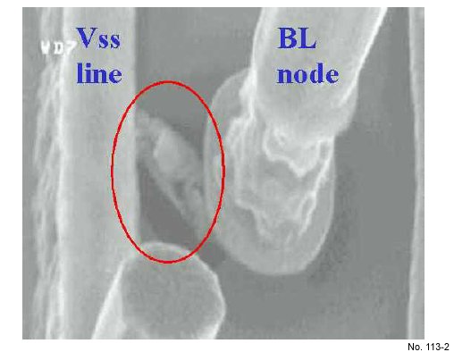
Figure 2: SEM image of photoemission located
metal residue between BL node and VSS-line.