Alphabetical Index
Browse by Elements
Keyword Search
Dry Etchants
Dry and Wet Etchants
Wet Etchants
Bulk Etchants
Layer Etchants
Nano Etchants
Single Crystal Etchants
Thin Film Etchants
Thin Foil Etchants
Wafer Etchants
Al Etchants
Cd Etchants
Ga Etchants
Ge Etchants
In Etchants
New Etchants
Other Etchants
Si Etchants
Zn Etchants
Help
Home
Metal Residue Between BL and VSS-Line III
Material Name: Silicon
Record No.: 114
Primary Chemical Element in Material: Si
Sample Type: Wafer
Uses: Etching
Etchant Name: None
Etching Method: Dry etching
Etchant (Electrolyte) Composition: No data
Procedure (Condition): No data
Note: The device is 0.15 µm process technology, 7-level
metal (4-7 layers are dummy layers) design 2Mb
synchronous SRAM with a single column failure.
The device presents high IDD leakage of 700~900
µA under 1.5V constant voltage.
After several attempts, neither front-side OBIRCH
nor front-side photoemisison microscope could
isolated the fault site due to dense metal layers. As a
result, liquid crystal analysis (LCA), which is a
very traditional technique, under specific range of
voltage bias was attempted to overcome this
difficulty (Fig 1, 2). The attached laser cutter also
provides an advantage to in-situ mark the fault site.
Reference: Cheng-Piao Lin, Cheng-Chun Ting, Chin-Hsin Tang, Cheng-Hsu Wu, Chih-Ming Kuo,
Yung-Sheng Huang, Application of Various Fault Localization Techniques to Different
Types of 6T-SRAM column Failures, ISTFA 2002, Proceedings of the 28th International Symposium for Testing and Failure Analysis, 3-7 November 2002, Phoenix Civic Center, Phoenix, Arizona, pp. 259-265.

Figure 1: Image of LCA hot spot and in-situ laser
mark.
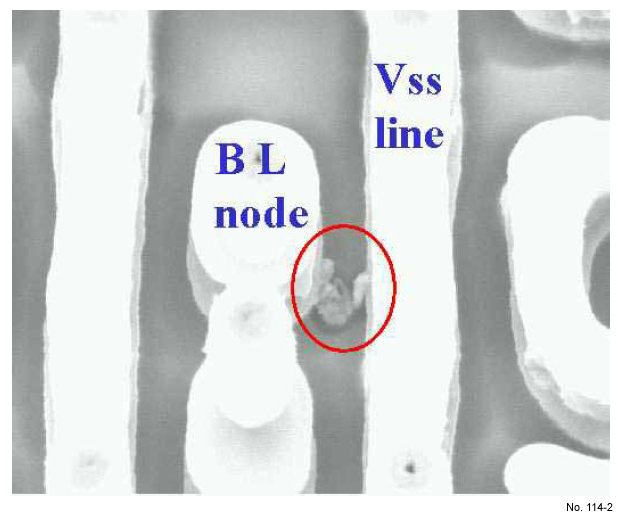
Figure 2: SEM image of LCA located metal residue between BL node and VSS-line.