Alphabetical Index
Browse by Elements
Keyword Search
Dry Etchants
Dry and Wet Etchants
Wet Etchants
Bulk Etchants
Layer Etchants
Nano Etchants
Single Crystal Etchants
Thin Film Etchants
Thin Foil Etchants
Wafer Etchants
Al Etchants
Cd Etchants
Ga Etchants
Ge Etchants
In Etchants
New Etchants
Other Etchants
Si Etchants
Zn Etchants
Help
Home
TiN-Rich Metal Flake Between BL and VSS-Line
Material Name: Silicon
Record No.: 115
Primary Chemical Element in Material: Si
Sample Type: Wafer
Uses: Etching
Etchant Name: None
Etching Method: Dry etching
Etchant (Electrolyte) Composition: No data
Procedure (Condition): No data
Note: This case shows that not all metallic short type of
defects induce high IDD leakage. The device is
0.25 µm process technology, 3-level metal design
1Mb synchronous SRAM with a single column
failure. The device presents low IDD leakage of
40~50 µA under 2.5V constant voltage.
For this case, we used a system where a photo
emission microscope was connected with a
engineering memory tester -Mosaid 3490. High repetition rates with active bias
condition can be more effective to locate the failure
site. The result is TiN-rich metal flake between BL
node and VSS-line (Fig. 1, 2). The composition of
metal flake also can explain why its resistance is
higher than other cases.
Reference: Cheng-Piao Lin, Cheng-Chun Ting, Chin-Hsin Tang, Cheng-Hsu Wu, Chih-Ming Kuo,
Yung-Sheng Huang, Application of Various Fault Localization Techniques to Different
Types of 6T-SRAM column Failures, ISTFA 2002, Proceedings of the 28th International Symposium for Testing and Failure Analysis, 3-7 November 2002, Phoenix Civic Center, Phoenix, Arizona, pp. 259-265.
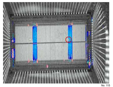
Figure 1: Photoemission image occurs by active
bias stress.
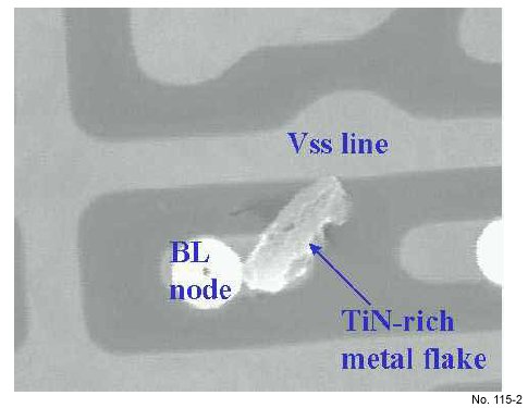
Figure 2: SEM image of photoemission located
TiN-rich metal flake between BL node and VSS-line.