Alphabetical Index
Browse by Elements
Keyword Search
Dry Etchants
Dry and Wet Etchants
Wet Etchants
Bulk Etchants
Layer Etchants
Nano Etchants
Single Crystal Etchants
Thin Film Etchants
Thin Foil Etchants
Wafer Etchants
Al Etchants
Cd Etchants
Ga Etchants
Ge Etchants
In Etchants
New Etchants
Other Etchants
Si Etchants
Zn Etchants
Help
Home
Metal Residue Between BL and VSS-Line IV
Material Name: Silicon
Record No.: 116
Primary Chemical Element in Material: Si
Sample Type: Wafer
Uses: Etching
Etchant Name: None
Etching Method: Dry etching
Etchant (Electrolyte) Composition: No data
Procedure (Condition): No data
Note: In this case, the device that was returned from our
customer is 0.15 µm process technology, 3-level
metal design 18-Mb synchronous SRAM with a
double column failure. The device presents normal
IDD leakage under 1.5V constant voltage. A short
between neighboring bitlines was suspected due to
its IDD level and layout.
Reference: Cheng-Piao Lin, Cheng-Chun Ting, Chin-Hsin Tang, Cheng-Hsu Wu, Chih-Ming Kuo,
Yung-Sheng Huang, Application of Various Fault Localization Techniques to Different
Types of 6T-SRAM column Failures, ISTFA 2002, Proceedings of the 28th International Symposium for Testing and Failure Analysis, 3-7 November 2002, Phoenix Civic Center, Phoenix, Arizona, pp. 259-265.
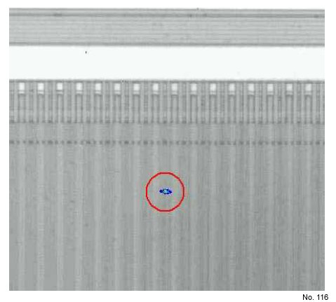
Figure 1: Photoemission image under simple write
operation mode.
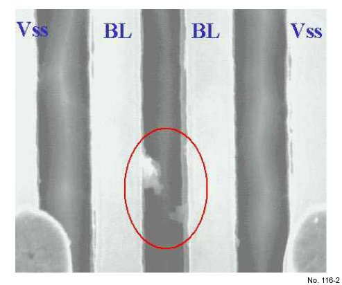
Figure 2: SEM image of photoemission located
metal residue between neighboring BLs.