Alphabetical Index
Browse by Elements
Keyword Search
Dry Etchants
Dry and Wet Etchants
Wet Etchants
Bulk Etchants
Layer Etchants
Nano Etchants
Single Crystal Etchants
Thin Film Etchants
Thin Foil Etchants
Wafer Etchants
Al Etchants
Cd Etchants
Ga Etchants
Ge Etchants
In Etchants
New Etchants
Other Etchants
Si Etchants
Zn Etchants
Help
Home
Missing Metal Pillars
Material Name: Silicon
Record No.: 117
Primary Chemical Element in Material: Si
Sample Type: Wafer
Uses: Etching
Etchant Name: None
Etching Method: Dry etching
Etchant (Electrolyte) Composition: No data
Procedure (Condition): No data
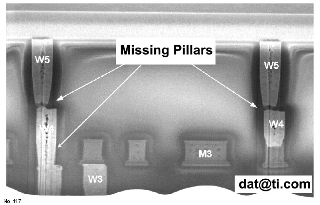
Note: Smaller technologies and increasing chip
functionality has resulted in tightly packed devices
and more stacked metal layers. For technologies
between 0.25 µm and 0.14 µm, stacking packed
metal layers required the combination of Tungsten
plugs as interconnection and the utilization of
Chemical Mechanical Polishing (CMP). “Pillar”,
however, is a small metal line, which allows interlevel
connections between Tungsten plugs. The
size and shape of the pillar can be a yield limiting
issue. The process of identification and resolution
of the missing metal pillar included yield analysis,
electrical and physical failure analysis, root cause
analysis and the engineering coordination of photo
engineering, etch process engineering, CMP
engineering, integration engineering, and inline
inspection. Resolving the missing pillar issue has
proven to have significant contribution to yield.
Reference: Dat Nguyen, et al., Missing Metal Pillar Failure Analysis-A Plug Technology Issue, ISTFA 2002, Proceedings of the 28th International Symposium for Testing and Failure Analysis, 3-7 November 2002, Phoenix Civic Center, Phoenix, Arizona, pp. 267-272.

Figure 1: Fault isolation found missing metal pillars.

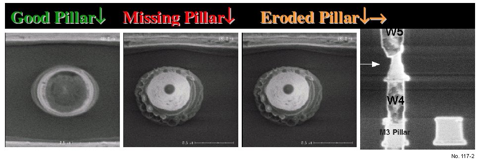
Figure 2: Pillar patterning and metallization.