Alphabetical Index
Browse by Elements
Keyword Search
Dry Etchants
Dry and Wet Etchants
Wet Etchants
Bulk Etchants
Layer Etchants
Nano Etchants
Single Crystal Etchants
Thin Film Etchants
Thin Foil Etchants
Wafer Etchants
Al Etchants
Cd Etchants
Ga Etchants
Ge Etchants
In Etchants
New Etchants
Other Etchants
Si Etchants
Zn Etchants
Help
Home
Defect in Digital Micromirror Device
Material Name: Silicon
Record No.: 118
Primary Chemical Element in Material: Si
Sample Type: Wafer
Uses: Etching
Etchant Name: None
Etching Method: Dry etching
Etchant (Electrolyte) Composition: No data
Procedure (Condition): No data
Note: Figure 1 shows just such
trapped carbon-based material that caused the final
image to be less than acceptable. As light travels
through the window, a shadow of the material is cast upon the surface of the mirrors. This shadow is also
transmitted back to the window in reflection, and
therefore is a problem in at least two occurrences. If
the window is observed using a directional light
source that is approaching the unit at an angle
similar to that used in the actual application, a pair
of dark or bright spots will be observed. The window must be removed mechanically before
further analysis is possible within the device. This is
accomplished using methods dependent upon the
type package used. Grinding through seam welds is
the most common method. Extreme care must be
taken to prevent grinding into the operational cavity,
as this will distribute metal particles freely
throughout that cavity and cloud the analysis.
The superstructure required to build a DMD is a 3-D
array of metal and hollow space. Fig. 2 shows this
as seen from an extreme viewing angle.
Removal of the mirrors can be carried out by several
methods, but the most common method is exquisite
in its simplicity. Common transparent adhesive tape
is applied carefully to the surface of the mirrors with
a light amount of pressure, then removed in one
motion. With the tape come the mirrors, breaking
the hinges in the process. The view of the
substructure surface is now unobstructed, and on
the tape we removed are all of the mirrors and yokes
available for inspection in an inverted position as in
Figure 4. This image shows the entire area of mirrors removed
using the tape, and an expanded view of a single
yoke/mirror assembly. This is the view offered by
inspecting the rear of the mirrors, usually with a low
accelerating voltage in a Field Emission SEM.
This allows us to inspect the lower surfaces of both
the yokes and mirrors. If reasonable care is taken,
no damage of the substructure surface is observed.
Removal of only the mirrors without damaging the
yokes requires a bit more finesse, and also an
isotropic dry etch. While this is still a global
approach much like the transparent tape method, it
will fold the mirrors and leave the yoke assembly
available for inspection and analysis. This approach
is seen in Figure 6. Similar results are obtainable
using a laser-cutting tool for removing one or more
mirrors. There is some variation in laser power
between units, and therefore each setup must be
worked with to obtain the optimum power and spot
size for single pulse laser mirror removal.
Reference: Cary Davis,Wes Mahin, and Becky Holdford, Failure Analysis of the Digital Micromirror Device, ISTFA 2002, Proceedings of the 28th International Symposium for Testing and Failure Analysis, 3-7 November 2002, Phoenix Civic Center, Phoenix, Arizona, pp. 291-294.
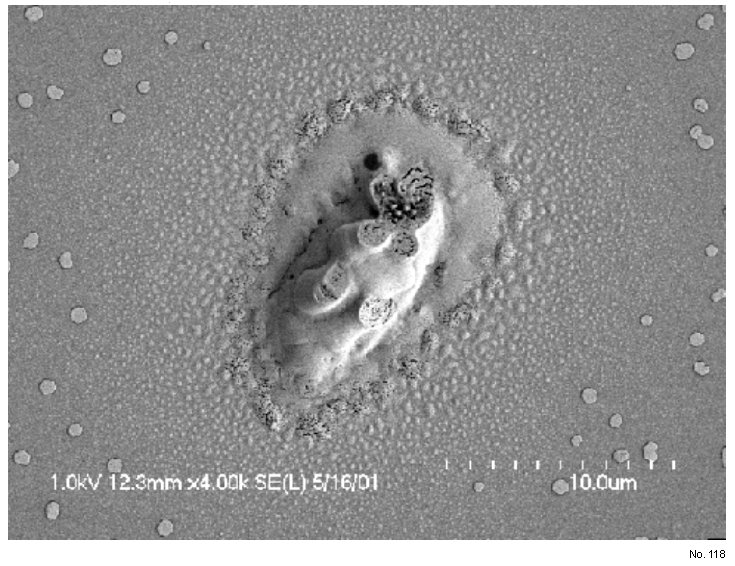
Figure 1: Carbon material which has dried on the
surface of the window.
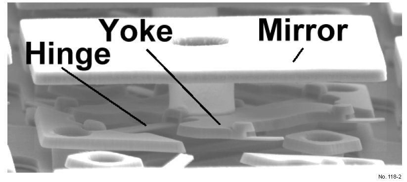
Figure 2: Typical pixel as seen from extreme viewing
angle.
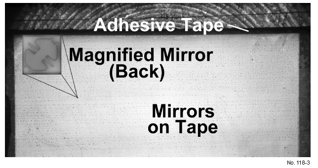
Figure 4: Tape after mirror removal.
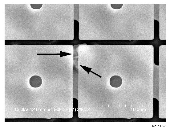
Figure 5: View of material trapped behind the mirror
imaged using High Acceleration Imaging.
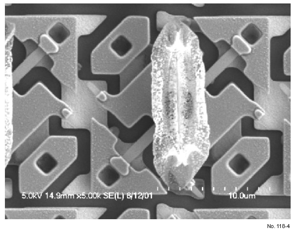
Figure 6: Mirror reduced using RIE isotropic etch.