Alphabetical Index
Browse by Elements
Keyword Search
Dry Etchants
Dry and Wet Etchants
Wet Etchants
Bulk Etchants
Layer Etchants
Nano Etchants
Single Crystal Etchants
Thin Film Etchants
Thin Foil Etchants
Wafer Etchants
Al Etchants
Cd Etchants
Ga Etchants
Ge Etchants
In Etchants
New Etchants
Other Etchants
Si Etchants
Zn Etchants
Help
Home
Breakdown in Vertical Gate Oxide
Material Name: Silicon
Record No.: 119
Primary Chemical Element in Material: Si
Sample Type: Wafer
Uses: Etching
Etchant Name: None
Etching Method: Wet etching
Etchant (Electrolyte) Composition: No data
Procedure (Condition): No data
Note: The stress leakage current data does not provide any
location information of the failing transistors. The
PFA flow has to start with localization of the gate
oxide breakdown site. The widely used
photoemission microscopy is used here along with
electrical probing to narrow down the failure site
within some (3-5) transistors along one word line.
Figure 5 shows a photoemission image example.
The sample preparation starts from delayering the
array to the bit line level using mechanical polishing
and etching. Reactive ion etching (RIE) is then used
to remove the dielectric between the bit lines. RIE
etching is necessary here in order to make the word
lines visible in the FIB tool. Alternatively the sample
can be delayered to the word line level, but the area
of interest must be capped with metal to avoid any
damage of the polysilicon within the gate during the
following wet etch. With the limited number of
samples that were processed so far the second
approach resulted in better quality SEM images. The
next step is to remove materials on both sides of the
word line connecting the failing cell through FIB
milling.
A Micrion 9000 FIB was used to perform two crosssections
on both sides of the wordline, as shown in
Figure 6. The figure shows a cross-sectional view of
a vertical transistor cell. This cross section is not part
of the here described preparation flow for the vertical
transistor. It illustrates were the cross-sections which
are used for the vertical transistor remove material
(hatched areas) in order to access the vertical gate
oxide. Figure 6 shows also the range where the actual
cross section can be located (arrow). This range is
about three times as wide as the minimum feature
size since it is only necessary to cut in between two
vertical gates. The remaining silicon is removed by a
wet etch. The material removal was performed with a
step mill followed by a single pass mill, both using a
100pA beam current. The milling box size was in the
range of 3ìm by 3ìm. Since the space between two
trenches is 3 times the minimum feature size (range
of successful cross-section), this cross-section
operation is believed to be applicable down to 110nm
minimum feature size without problems. The final
stage of the preparation is to remove the silicon
surrounding the trenches so that the gate oxide is
exposed for SEM examination. Chemical solution
HNO3:HF (100:1) wet etch was used. Typical etch
time is between 5 and 20 seconds depending on the
location of the FIB cuts. The etch process can be
done in iterations with SEM inspection to find the
exact etch time. The exposed oxide surfaces were
shown to be able to sustain several seconds of
overetching without any visible damages. Past
experience with this etch proofed to be selective
enough and very reliable to expose thin oxides from
Silicon. Figure 7 shows the sample after wet
etching. The vertical transistors along one wordline
are completely exposed. Since multiple transistors
along one wordline can easily be exposed, an exact
prelocalization of the failing transistor is not required
in this direction. Perpendicular to the wordline the
location information is crucial for the success of the
described preparation technique since adjacent word
lines are removed.
Figure 8 and Figure 9 show a pinhole in the vertical
gate oxide exposed after the described sample
preparation. The gate oxide breakdown spot is not
correlated to any interfaces, which provides
important information for further process
improvements. The dark decoration of the failing gate oxide is
caused by an etch-out effect. The HNO3:HF (100:1)
wet etch reached the gate poly-silicon through the pinhole and etched out some of the poly-silicon
around the pinhole within the gate – leaving a cavity
there. This cavity reduced the secondary electron
emission rate and thus caused the darker appearance
of the failing gate. This is a typical result as expected
for intrinsic gate oxide fails.
Reference: Michael W. Ruprecht, et al., Sample preparation for vertical transistors in DRAM, ISTFA 2002, Proceedings of the 28th International Symposium for Testing and Failure Analysis, 3-7 November 2002, Phoenix Civic Center, Phoenix, Arizona, pp. 307-311.
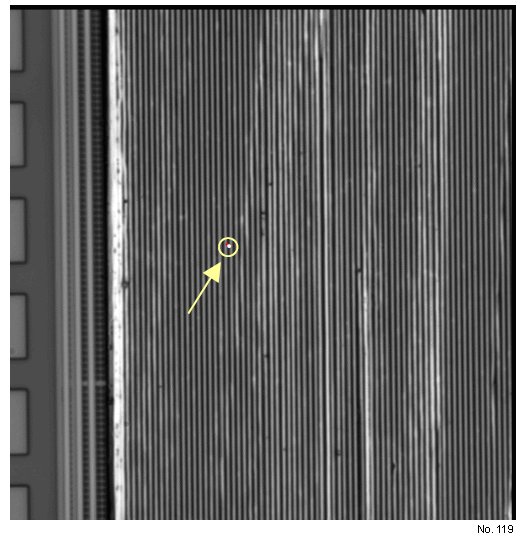
Figure 5: Photo emission image of gate oxide
breakdown in DRAM array. The emission spot is
visible inside the circled area.

Figure 6: Cross-section of vertical access transistor in
DRAM array.

Figure 7: Exposed vertical transistors after wet
chemical etch.
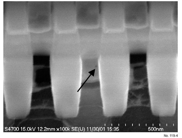
Figure 8: Breakdown in vertical gate oxide.
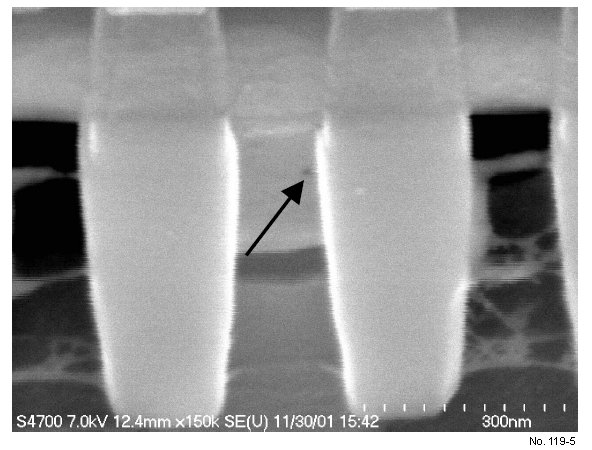
Figure 9: Higher magnification of gate oxide
breakdown shown in Figure 8.