Alphabetical Index
Browse by Elements
Keyword Search
Dry Etchants
Dry and Wet Etchants
Wet Etchants
Bulk Etchants
Layer Etchants
Nano Etchants
Single Crystal Etchants
Thin Film Etchants
Thin Foil Etchants
Wafer Etchants
Al Etchants
Cd Etchants
Ga Etchants
Ge Etchants
In Etchants
New Etchants
Other Etchants
Si Etchants
Zn Etchants
Help
Home
Tungsten (W) Plugs
Material Name: Silicon
Record No.: 121
Primary Chemical Element in Material: Si
Sample Type: Wafer
Uses: Etching
Etchant Name: None
Etching Method: Dry etching
Etchant (Electrolyte) Composition: No data
Procedure (Condition): No data
Note: The modified BT process can provide more over-etch margin for the variation of
dielectric layers during CMP step since the gas chemistries etch away both oxide and
TiN layers. In order to break-through TiN completely and gentlely, lower power,
higher pressure, and longer etching time are also applied during modified BT step.
Figure 1 shows the cross-sections of via after W plugs deposited by using same gas
chemistries in both main etching and BT steps. The taper angle of via profile is
around 88.6°, CD bias that means the difference between DICD and FICD is about
0.01 ìm, the Aluminum (Al) gauging is about 58 nm.
The third approach is also investigated for TiN break-through step by using SF6
gas chemistry. Much lower power, higher pressure, shorter etching time compared to
main etching are applied for the SF6 break-through step. However, this process
causes too much Al gauging which increases the contact resistance. Figure 2 shows
the cross-section of via profile for SF6 process after W plugs deposited. Finally, the
C4F8 TiN break-through process shows the least contact resistance among the three
different approaches on several split lots. Therefore, this process is fixed inline as the
POR process for TiN break-through application. All of the above work is completed
on the development tool.
Reference: JUAN JUAN WANG, ADVANCED PLASMA-ETCHING PROCESSES FOR DIELECTRIC MATERIALS IN VLSI TECHNOLOGY, PhD Thesis, UNIVERSITY OF FLORIDA, 2002, pp. 60-62.
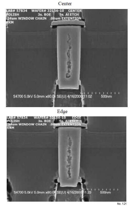
Figure 1: Cross-sections of Break-through (BT) process after Tungsten (W) plugs deposited.
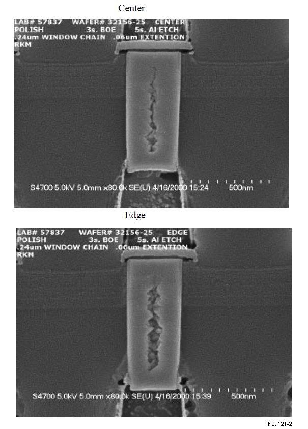
Figure 2: Cross-sections of Break-through (BT) process after Tungsten (W) plugs deposited