Alphabetical Index
Browse by Elements
Keyword Search
Dry Etchants
Dry and Wet Etchants
Wet Etchants
Bulk Etchants
Layer Etchants
Nano Etchants
Single Crystal Etchants
Thin Film Etchants
Thin Foil Etchants
Wafer Etchants
Al Etchants
Cd Etchants
Ga Etchants
Ge Etchants
In Etchants
New Etchants
Other Etchants
Si Etchants
Zn Etchants
Help
Home
Misalignment
Material Name: TiN
Record No.: 122
Primary Chemical Element in Material: Ti
Sample Type: Layer
Uses: Etching
Etchant Name: None
Etching Method: Dry etching
Etchant (Electrolyte) Composition: No data
Procedure (Condition): No data
Note: Baseline Recipe: The baseline recipe for the “Stop on TiN” process is set up as the following:
SPARC etch step, Main Etching step. It is also called one step etching process since the
over etching is included in the Main Etching step.
During Main etching step, higher chuck temperature, lower power are explored to
get higher selectivity of oxide to TiN in the beginning of development work. In addition,
the thickness of TiN layer is doubled to have bigger etching process margin. Figure 1
shows the cross-sections of “Stop on TiN” baseline process. The via etching process is
stopped on the TiN layer successfully and the via profile is shaped straightly. The TiN gauging is around 12 nm/14 nm (center/edge) and equals 10% to 20% of the TiN
thickness. The CD bias is less than +/-0.01 µm that is very similar with the BT process.
40% to 50% over-etch without etch stop is obtained from the cross-section SEM pictures
on 18 kA wafers. Much higher selectivity of oxide over TiN is up to 32:1 during the
baseline process. It is very interesting to find another issue relative to the process margin
of the photolithography step after the wafer is etched with the baseline etch recipe. The
TiN layer is broken through at the corner of the vias due to the misalignment of the vias.
The chance for the failure of EM is increased dramatically as the break-through process
did before. Figure 2 shows the cross-section SEM pictures for the misalignment vias
after etching and PR strip. Figure 36 shows the cross-section SEM pictures for the same
misalignment vias after W plugs deposited. Both of them obviously indicated that the
misalignment issue should be addressed before the lots go to via etch step. This problem
is solved smoothly after the photo engineers adjust the process margin and reset up the
speciation of the misalignment.
The special experiment is completed to check the etch rate of TiN during main
etching. The method used in here is to have the difference of TiN gauging be divided by
the difference of etch times. At first, some special mechanical wafers need to be prepared
for the experiments. The bare Si wafers are used in here to reduce the development cost.
The 1000 Å TiN layer is deposited on the Si wafers instead of standard TiN thickness.
Then the wafers go through the standard Via Zone Test (VIAZT) routing to have the
regular dielectric layer deposition and the standard photolithography process. The
advantage of these mechanical wafers is that they are very similar with the actual VIAZT
wafers except thicker TiN layer. The more accurate data can be collected on these wafers.
Finally, one mechanical wafer is etched by using the baseline “Stop on TiN”
process, another mechanical wafer is etched one more extra minute compared to the
previous wafer. The difference of TiN gauging can be read accurately from the crosssection
SEM pictures of these two wafers by using the PCI software. The etch rate of TiN
can be calculated by the quotient of the difference of TiN gauging over one minute. The
final TiN etch rate is about 150 Å/min which is very slow compared to the etch rate of
oxide during the main etching. The selectivity of oxide over TiN is obtained after the etch
rate of oxide is divided by the etch rate of TiN.
Reference: JUAN JUAN WANG, ADVANCED PLASMA-ETCHING PROCESSES FOR DIELECTRIC MATERIALS IN VLSI TECHNOLOGY, PhD Thesis, UNIVERSITY OF FLORIDA, 2002, pp. 64-68.

Figure 1: Cross-sections of “Stop on TiN” baseline process.
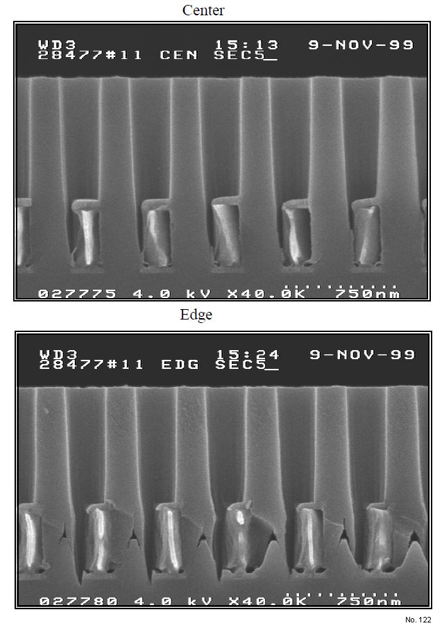
Figure 2: Cross-sections of “Stop on TiN” baseline process for the misalignment vias
after etching.
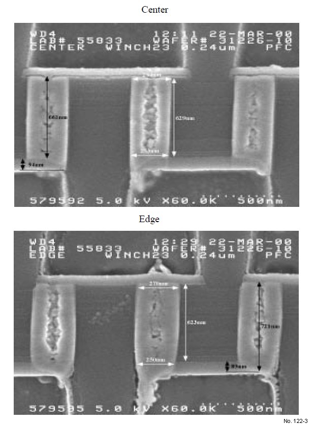
Figure 2: Cross-sections of “Stop on TiN” baseline process for the misalignment vias
after W plugs deposited.