Alphabetical Index
Browse by Elements
Keyword Search
Dry Etchants
Dry and Wet Etchants
Wet Etchants
Bulk Etchants
Layer Etchants
Nano Etchants
Single Crystal Etchants
Thin Film Etchants
Thin Foil Etchants
Wafer Etchants
Al Etchants
Cd Etchants
Ga Etchants
Ge Etchants
In Etchants
New Etchants
Other Etchants
Si Etchants
Zn Etchants
Help
Home
Carbon Contamination
Material Name: Carbon
Record No.: 123
Primary Chemical Element in Material: C
Sample Type: Wafer
Uses: Contamination
Etchant Name: None
Etching Method: Dry etching
Etchant (Electrolyte) Composition: No data
Procedure (Condition): No data
Note: Organic (H and C containing materials) contaminants arrive at wafer surfaces from diverse
sources: (1) photo resist out gassing products as vapors and as de laminated particles from
organic accumulation on beam line surfaces, (2) residue from "clea ning" products used in
periodic maintenance of end station chambers, (3) out gassing and abrasion wear products from
O rings and other seals, (4) elements from "vacuum lubricants" used on moving machine parts
and (5) contact transfers from wafer "heat sink s" (which often contain metals and organic
materials to enhance elastomer adhesion to wafer backsides and thermal conductivity).
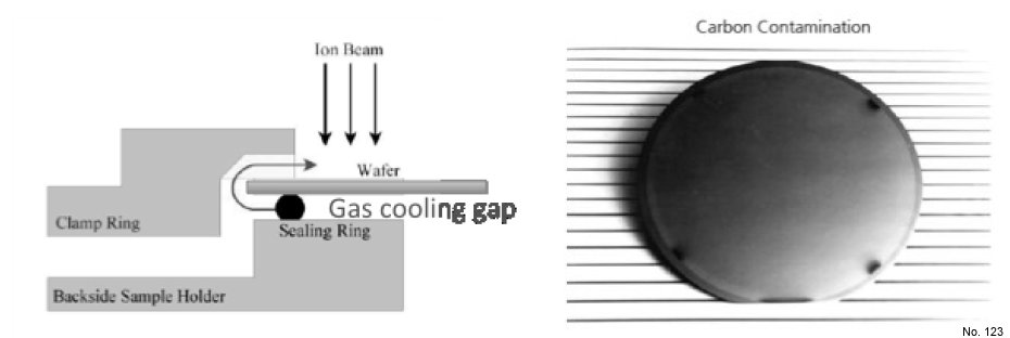
In the example shown in Fig.1, a Teflon O ring seal on a gas cooled wafer fixture was over
heated by the incident ion bea m and out gassed onto the wafer surface area. The ion beam then
cross linked the organic residue onto the wafer surface.
Lubricants for moving parts throughout the implanter vacuum system can be an uncontrolled
source of diverse elements, including many that are usually "bann ed" from use in IC fabrication.
A survey of elemental composition in a variety of "vendor certified" lubricants ( Fig.12 4.10)
shows many examples of high metal (Al, Zn) and alkali (Na, Ca, Li) elements. An additional
complication is that lubricants that are approved for use for atmospheric conditions can be
accidentally used as vacuum lubricants leading to excessive vapor pressures in vacuum and the
presence of diverse and potentially harmful (to semiconductor devices) elements.
Reference: Michael I. Current, Heiner Ryssel, Chapter 12, Ion Beam Purity and Wafer Contamination, ResearchGate, 2018, https://www.researchgate.net/publication/330357088, p. 27.

Figure 1: Organic flow path (left) for an over heated Teflon O ring seal for a gas cooled
wafer fixture and photo (r ight) of C residues cross linked by the incident ion beam on the wafer
front surface
Table 1: Elemental analysis of a variety of "vendor certified" lubricants for ion
implantation systems.
