Alphabetical Index
Browse by Elements
Keyword Search
Dry Etchants
Dry and Wet Etchants
Wet Etchants
Bulk Etchants
Layer Etchants
Nano Etchants
Single Crystal Etchants
Thin Film Etchants
Thin Foil Etchants
Wafer Etchants
Al Etchants
Cd Etchants
Ga Etchants
Ge Etchants
In Etchants
New Etchants
Other Etchants
Si Etchants
Zn Etchants
Help
Home
Wafer Spinning Rate
Material Name: Silicon
Record No.: 124
Primary Chemical Element in Material: Si
Sample Type: Wafer
Uses: Contamination
Etchant Name: None
Etching Method: Dry etching
Etchant (Electrolyte) Composition: No data
Procedure (Condition): No data
Note: In addition to blocking ion paths into target surfaces, the arrival of
particles onto the surface of rapidly moving wafer s can cause serious impact damage to fine
featured IC device structures (Fig.1). For 200 mm wafers on a spinning wheel with a 1200
mm radius to the wafer center and a 1250 rpm rotation rate, the lateral wafer motion is ~83 m/s.
The impact of a part icle on <0.25 µm wide poly Si lines is sufficient to shatter the structures,
with the extent of damage increasing for smaller device dimensions.
Reference: Michael I. Current, Heiner Ryssel, Chapter 12, Ion Beam Purity and Wafer Contamination, ResearchGate, 2018, https://www.researchgate.net/publication/330357088, pp. 31-32.
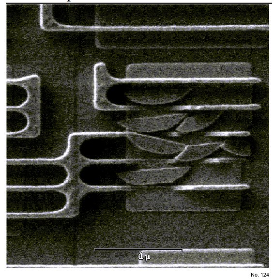
Figure 1: Damage to 100 nm wide poly Si lines from particle impacts on a wafer
spinning at ~83 m/s on a spinning wheel end station.