Alphabetical Index
Browse by Elements
Keyword Search
Dry Etchants
Dry and Wet Etchants
Wet Etchants
Bulk Etchants
Layer Etchants
Nano Etchants
Single Crystal Etchants
Thin Film Etchants
Thin Foil Etchants
Wafer Etchants
Al Etchants
Cd Etchants
Ga Etchants
Ge Etchants
In Etchants
New Etchants
Other Etchants
Si Etchants
Zn Etchants
Help
Home
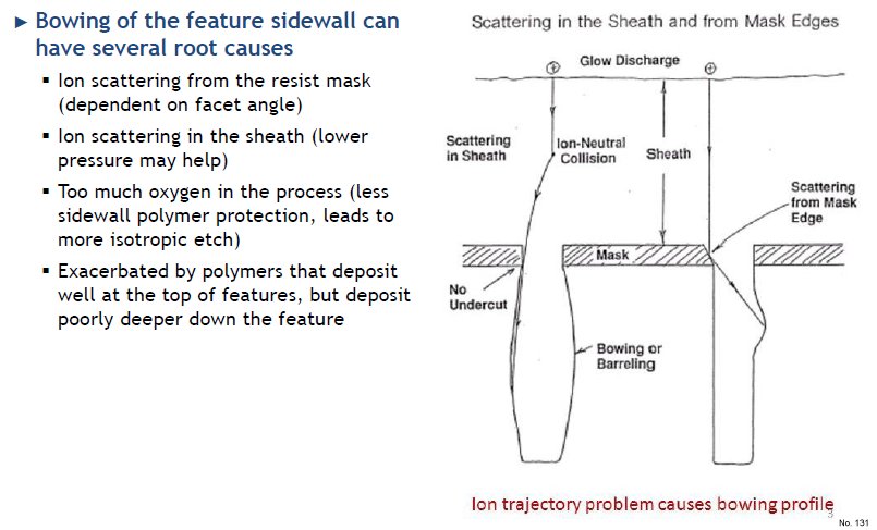
Bowing
Material Name: Silicon
Record No.: 131
Primary Chemical Element in Material: Si
Sample Type: Wafer
Uses: Etching
Etchant Name: None
Etching Method: Dry etching
Etchant (Electrolyte) Composition: No data
Procedure (Condition): No data
Note: Bowing of the feature sidewall can have several root causes
- Ion scattering from the resist mask
(dependent on facet.
- Ion scattering in the sheath (lower
pressure may help).
- Too much oxygen in the process (less
sidewall polymer protection, leads to
more isotropic etch).
- Exacerbated by polymers that deposit
well at the top of features, but deposit
poorly deeper down the feature.
Reference: Steve Sirard, Introduction to Plasma Etching, Lam Research Corporation, PowerPoint Presentation, https://docplayer.net, 2020, pp. 1-58.

Figure 1: Bowing.