Alphabetical Index
Browse by Elements
Keyword Search
Dry Etchants
Dry and Wet Etchants
Wet Etchants
Bulk Etchants
Layer Etchants
Nano Etchants
Single Crystal Etchants
Thin Film Etchants
Thin Foil Etchants
Wafer Etchants
Al Etchants
Cd Etchants
Ga Etchants
Ge Etchants
In Etchants
New Etchants
Other Etchants
Si Etchants
Zn Etchants
Help
Home
Striations
Material Name: Silicon
Record No.: 133
Primary Chemical Element in Material: Si
Sample Type: Wafer
Uses: Etching
Etchant Name: None
Etching Method: Dry etching
Etchant (Electrolyte) Composition: No data
Procedure (Condition): No data
Note:
- Extended roughness on the sidewalls of etched features
- Seen on both holes and trenches
- Due to roughness/striation formation in the resist being transferred to underlayers
- Exacerbated with 193 nm resists
- Likely related to how plasma modifies the resists at different length scales
- Ions impact ~2 nm of surface, causing graphitic densified region
- VUV radiation may either chain scission or cross link at deeper depths (~100 nm)
- Different mechanical properties of modified layers can lead to resist buckling or roughening
Reference: Steve Sirard, Introduction to Plasma Etching, Lam Research Corporation, PowerPoint Presentation, https://docplayer.net, 2020, pp. 1-58.
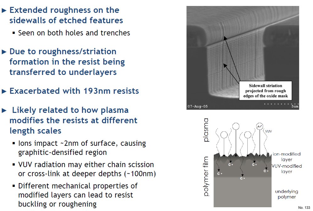
Figure 1: Striations.