Alphabetical Index
Browse by Elements
Keyword Search
Dry Etchants
Dry and Wet Etchants
Wet Etchants
Bulk Etchants
Layer Etchants
Nano Etchants
Single Crystal Etchants
Thin Film Etchants
Thin Foil Etchants
Wafer Etchants
Al Etchants
Cd Etchants
Ga Etchants
Ge Etchants
In Etchants
New Etchants
Other Etchants
Si Etchants
Zn Etchants
Help
Home
Voids - Germanium
Material Name: Germanium
Record No.: 149
Primary Chemical Element in Material: Ge
Sample Type: Wafer
Uses: Etching
Etchant Name: None
Etching Method: Dry etching
Etchant (Electrolyte) Composition: No data
Procedure (Condition): No data
Note: Figure 1 a) shows a TEM image from an array of wide Ge fins where the top
120 nm of the structures was amorphized due to the implantation. In this part of the
experiment the fins are approximately 450 nm tall and 105 nm wide. Narrow fins
with 20-25 nm width were completely amorphized under the same implant
conditions. In the following, bright-field TEM images homogeneous gray regions
are amorphous Ge and dark features are defects. The shown images are a
representative selection of a larger set of images. The intrinsic Ge recrystallization
rate is ~ 2 nm/s for 400 °C anneal, therefore after 3 minutes all the Ge is
expected to be recrystallized. Fins are partially amorphized on the top and in the
trench. Deposited carbon and platinum layers are also seen in the image. Figure 1 b) illustrates the fins after a 400 °C 3 min anneal where SPE is complete.
Reference: Maryam Shayesteh, Novel Processes, Test Structures and Characterisation for Future Germanium Technologie, PhD Thesis, NationalUniversityof Ireland, Cork, 2014, p. 117.
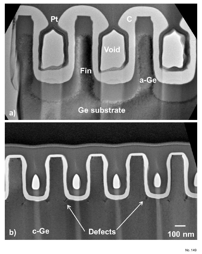
Figure 1: XTEM image of Ge fins, a) partially amorphized after implant. b) Although SPE is
complete, defects and twin boundaries are generated.