Alphabetical Index
Browse by Elements
Keyword Search
Dry Etchants
Dry and Wet Etchants
Wet Etchants
Bulk Etchants
Layer Etchants
Nano Etchants
Single Crystal Etchants
Thin Film Etchants
Thin Foil Etchants
Wafer Etchants
Al Etchants
Cd Etchants
Ga Etchants
Ge Etchants
In Etchants
New Etchants
Other Etchants
Si Etchants
Zn Etchants
Help
Home
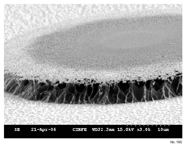
Pinholes Developed in the SiO2
Material Name: SiO2
Record No.: 160
Primary Chemical Element in Material: Si
Sample Type: Layer
Uses: Etching
Etchant Name: None
Etching Method: Dry etching
Etchant (Electrolyte) Composition: No data
Procedure (Condition): No data
Note: No data
Reference: Owen Cherry, Fabrication of an Atom Chip for Rydberg Atom-Metal SurfaceInteraction Studies, MSc Thesis, University of Waterloo, Ontario, 2007, p. 109.

Figure 1: SEM image of a polyimide PI 2611 film etched in O2 using a SiO2 etch mask. During the
etch, pinholes developed in the SiO2, causing a highly undercut film with rough edges. An Al etch
mask consitently gives smooth edges with less undercut.