Alphabetical Index
Browse by Elements
Keyword Search
Dry Etchants
Dry and Wet Etchants
Wet Etchants
Bulk Etchants
Layer Etchants
Nano Etchants
Single Crystal Etchants
Thin Film Etchants
Thin Foil Etchants
Wafer Etchants
Al Etchants
Cd Etchants
Ga Etchants
Ge Etchants
In Etchants
New Etchants
Other Etchants
Si Etchants
Zn Etchants
Help
Home
Poor Salicide Coverage
Material Name: Silicon
Record No.: 164
Primary Chemical Element in Material: Si
Sample Type: Wafer
Uses: Etching
Etchant Name: None
Etching Method: Wet etching
Etchant (Electrolyte) Composition: No data
Procedure (Condition): No data
Note: While developing a new salicide for a CMOS
manufacturing process, this technique proved to be
helpful in solving some initial yield problems.
Front-side analysis was difficult because floating
away the metal layers with HF often destroyed the
salicide before it could be inspected. The backside
technique, however, allowed selective removal of
the bulk silicon without compromising the layer of
salicide. Once the bulk silicon was removed,
islands of shallow trench isolation (STI) remained.
The layers of salicide and the gate oxides located between the STI layers remained intact. The
selectivity of the TMAH left the salicide
undamaged as seen in Figures 1 and 2.
Reference: Seth Prejean, Victoria Bruce, Joyce Burke, CMOS Backside Deprocessing With TMAH / IPA as a Sample
Preparation Procedure for Failure Analysis, ISTFA 2002, Proceedings of the 28th International Symposium for Testing and Failure Analysis, 3-7 November 2002, Phoenix Civic Center, Phoenix, Arizona, pp. 370-323.

Figure 1: Backside of transistor with poor salicide
coverage.
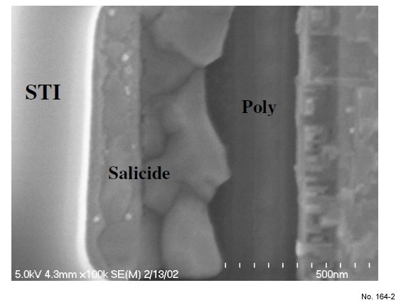
Figure 2: Non-uniform salicide grain formation
from the backside.