Alphabetical Index
Browse by Elements
Keyword Search
Dry Etchants
Dry and Wet Etchants
Wet Etchants
Bulk Etchants
Layer Etchants
Nano Etchants
Single Crystal Etchants
Thin Film Etchants
Thin Foil Etchants
Wafer Etchants
Al Etchants
Cd Etchants
Ga Etchants
Ge Etchants
In Etchants
New Etchants
Other Etchants
Si Etchants
Zn Etchants
Help
Home
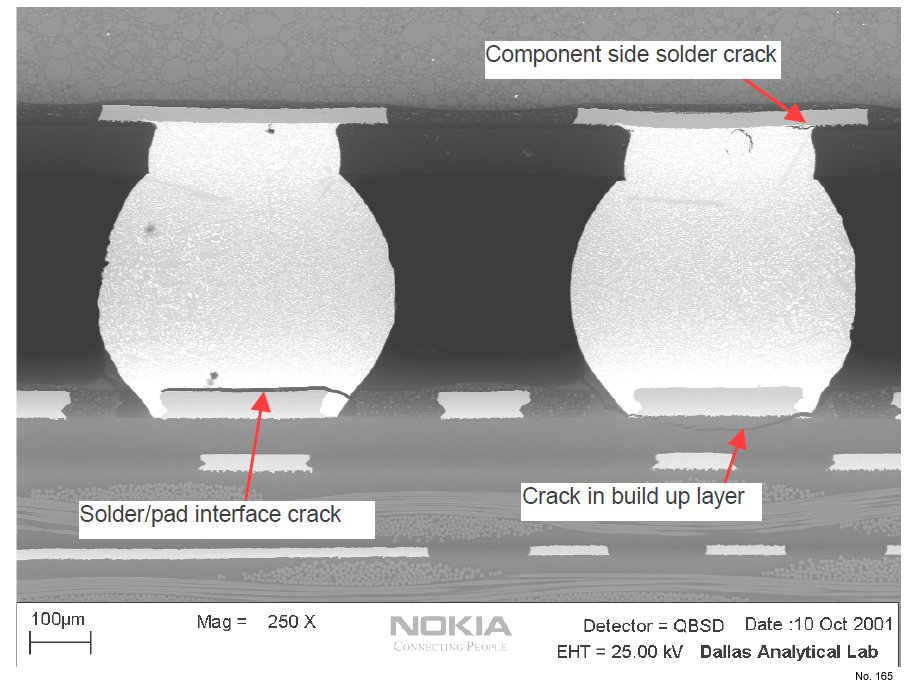
Solder/Pad Interface Crack
Material Name: Solder
Record No.: 164
Primary Chemical Element in Material: (Cu)
Sample Type: Wafer
Uses: Etching
Etchant Name: None
Etching Method: Wet etching
Etchant (Electrolyte) Composition: No data
Procedure (Condition): No data
Note: No data
Reference: Sridhar Canumalla, Santosh Shetty and Nael Hannan, Effect of Corner Underfill Voids on Chip Scale Package (CSP)
Performance under Mechanical Loading, ISTFA 2002, Proceedings of the 28th International Symposium for Testing and Failure Analysis, 3-7 November 2002, Phoenix Civic Center, Phoenix, Arizona, pp. 361-370.

Figure 1: Image of an improperly underfilled sample that failed in the simulated end use test is representative of the
population. Cracks were observed under the pad, at the solder/pad interface and in the solder near the component.