Alphabetical Index
Browse by Elements
Keyword Search
Dry Etchants
Dry and Wet Etchants
Wet Etchants
Bulk Etchants
Layer Etchants
Nano Etchants
Single Crystal Etchants
Thin Film Etchants
Thin Foil Etchants
Wafer Etchants
Al Etchants
Cd Etchants
Ga Etchants
Ge Etchants
In Etchants
New Etchants
Other Etchants
Si Etchants
Zn Etchants
Help
Home
Process Defect
Material Name: Solder
Record No.: 166
Primary Chemical Element in Material: (Cu)
Sample Type: Wafer
Uses: Etching
Etchant Name: None
Etching Method: Wet etching
Etchant (Electrolyte) Composition: No data
Procedure (Condition): No data
Note: A top view SEM image of the process defect is shown
in Figure 8. This SEM image was rotated by 90 degree
comparing to the microscopic image as shown in
Figure 6.
Reference: William Xia, Leakage Isolation of Mixed-Signal Devices at Operating Modes, ISTFA 2002, Proceedings of the 28th International Symposium for Testing and Failure Analysis, 3-7 November 2002, Phoenix Civic Center, Phoenix, Arizona, pp. 371-376.

Figure 7: As a comparison to device B, the same
area was shown (as pointed by an arrow) from a
known good device (without the process defect as
observed in device B).
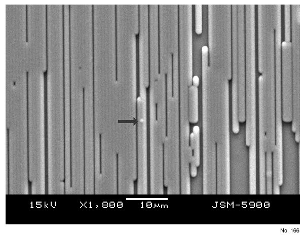
Figure 8: SEM photo of the process defect (as
pointed by an arrow) at the emission site for
device B). This SEM photo was rotated by 90
degree comparing to the microscopic image (in
Figure 6).
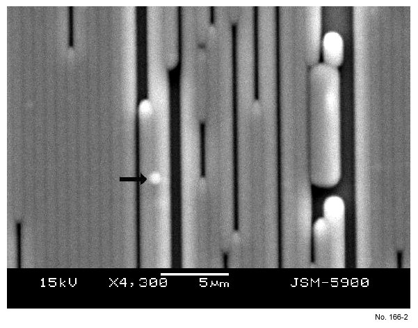
Figure 9: A closer look of the process defect at the
emission site for device B (as pointed by an
arrow), which was located between the two
narrowly spaced metal lines.
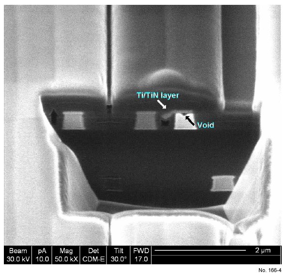
Figure 11: SEM image of the FIB cross-section at
the small process defect between the two adjacent
metal lines revealed a thin Ti/TiN barrier metal
stringer over the two narrowly spaced metal lines
and a void in aluminum metal under the Ti/TiN
layer (as pointed by the arrows).
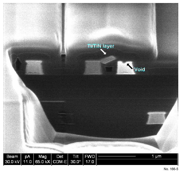
Figure 12: The Ti/TiN metal stringer was found to
extend over to the adjacent metal line on the left
side (as pointed by an arrow) as further FIB crosssectioning
was performed across the small process
defect.