Alphabetical Index
Browse by Elements
Keyword Search
Dry Etchants
Dry and Wet Etchants
Wet Etchants
Bulk Etchants
Layer Etchants
Nano Etchants
Single Crystal Etchants
Thin Film Etchants
Thin Foil Etchants
Wafer Etchants
Al Etchants
Cd Etchants
Ga Etchants
Ge Etchants
In Etchants
New Etchants
Other Etchants
Si Etchants
Zn Etchants
Help
Home
Voids in Solder Ball
Material Name: Solder
Record No.: 168
Primary Chemical Element in Material: (Cu)
Sample Type: Wafer
Uses: Etching
Etchant Name: None
Etching Method: Wet etching
Etchant (Electrolyte) Composition: No data
Procedure (Condition): No data
Note: No data
Reference: Sridhar Canumalla, Hee Dong Yang, and Puligandla Viswanadham, Method for Measuring Package to Board Interconnection Shear Strength
for Area Array, Fine Pitch Packages, ISTFA 2002, Proceedings of the 28th International Symposium for Testing and Failure Analysis, 3-7 November 2002, Phoenix Civic Center, Phoenix, Arizona, pp. 377-384.
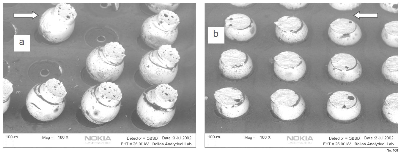
Figure 1: Scanning electron micrograph showing the location of the predominant fractures in a) C1 and b) C2.
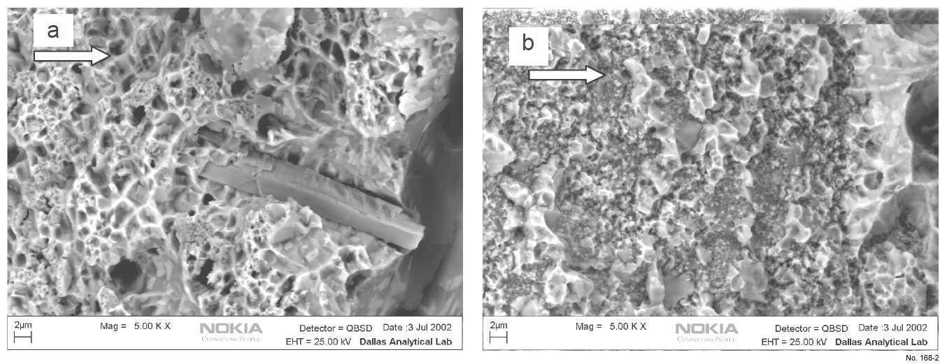
Figure 2: Dimples on a) solder ball side b) component pad side of a C1/S3 sample. These equiaxed dimples signifying
ductile fracture under a locally tensile stress field are observed on both sides of the fracture surface Arrows show the
direction of shearing force.