Alphabetical Index
Browse by Elements
Keyword Search
Dry Etchants
Dry and Wet Etchants
Wet Etchants
Bulk Etchants
Layer Etchants
Nano Etchants
Single Crystal Etchants
Thin Film Etchants
Thin Foil Etchants
Wafer Etchants
Al Etchants
Cd Etchants
Ga Etchants
Ge Etchants
In Etchants
New Etchants
Other Etchants
Si Etchants
Zn Etchants
Help
Home
Fluorine Contamination
Material Name: Wafer
Record No.: 172
Primary Chemical Element in Material: No data
Sample Type: Wafer
Uses: Etching
Etchant Name: None
Etching Method: Dry etching
Etchant (Electrolyte) Composition: No data
Procedure (Condition): No data
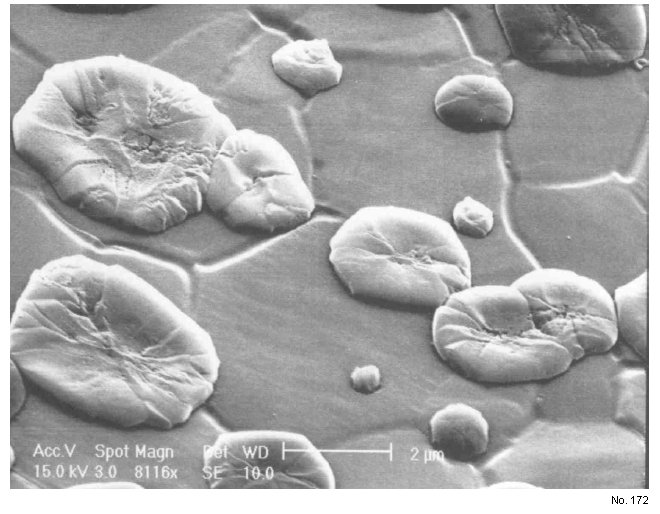
Note: SEM inspection revealed some "flower-like" defects on the affected
bondpads (Fig 1, SEM micrograph). EDX analysis
detected high fluorine peak on the "flower-like" defects on the affected bondpads (Fig 2, EDX
results).
Reference: Y. N. Hua, et al., A Study on Non-Stick Aluminium Bondpads due to Fluorine
Contamination using SEM, EDX, TEM, IC, AUGER,
XPS and TOF-SIMS Techniques, ISTFA 2002, Proceedings of the 28th International Symposium for Testing and Failure Analysis, 3-7 November 2002, Phoenix Civic Center, Phoenix, Arizona, pp. 495-504.

Figure 1: SEM micrograph shows the "flower-like "
defects with a planar-hexagonal structure.

Figure 2: EDX analysis showing high F peak detected
on the affected bondpad.