Alphabetical Index
Browse by Elements
Keyword Search
Dry Etchants
Dry and Wet Etchants
Wet Etchants
Bulk Etchants
Layer Etchants
Nano Etchants
Single Crystal Etchants
Thin Film Etchants
Thin Foil Etchants
Wafer Etchants
Al Etchants
Cd Etchants
Ga Etchants
Ge Etchants
In Etchants
New Etchants
Other Etchants
Si Etchants
Zn Etchants
Help
Home
Kirkendall’s Voids
Material Name: Solder
Record No.: 173
Primary Chemical Element in Material: Cu, Sn
Sample Type: Wafer
Uses: No data
Etchant Name: None
Etching Method: No data
Etchant (Electrolyte) Composition: No data
Procedure (Condition): No data
Note: Cross section TEM (XTEM) on the UBM pad
without solder showed the original Cu coating
thickness is about 500 nm. In the as-received
sample (which has already been reflowed once),
Cu layer has reacted to form Cu6Sn5 and Cu3Sn
compounds. The Cu3Sn phase is small grains
aggregated at the Ni(V) interface and mostly
within large Cu6Sn5 grains. Kirkendall voids are
accompanied and wrapped by Cu3Sn phase, as
shown in Fig 1. As reported previously, the
concave nature of the Cu6Sn5/Cu3Sn interface
strongly suggested the reaction is going toward
the Cu6Sn5 phase. Samples after reflow up to
10X did not show any major change in
microstructure. Both Cu6Sn5 and Cu3Sn
remained after 10 reflow cycles.
Reference: Chih-Hang Tung, et al., Microstructure Studies of Under Bump Metallization Systems
Using Transmission Electron Microscopy, ISTFA 2002, Proceedings of the 28th International Symposium for Testing and Failure Analysis, 3-7 November 2002, Phoenix Civic Center, Phoenix, Arizona, pp. 505-511.
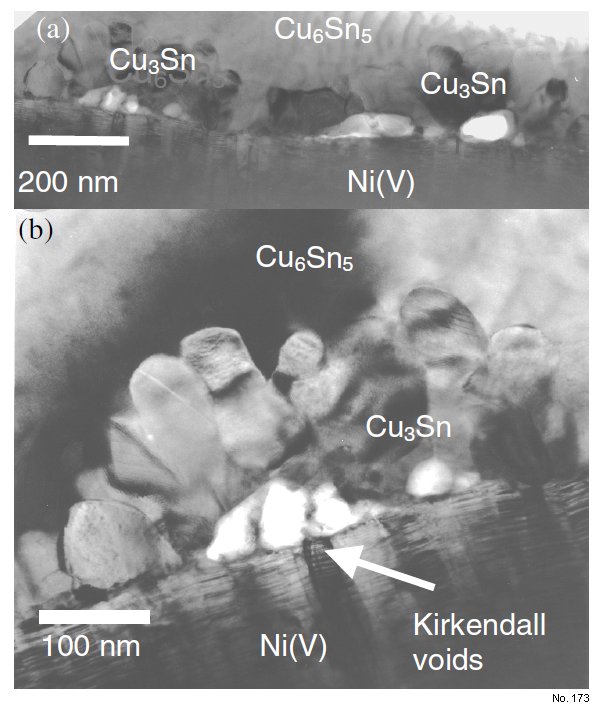
Figure 1: Cross section TEM on the as reflow Ni(V) UBM system showing Cu6Sn5, Cu3Sn intermetallics, and Kirkendall’s voids.