Alphabetical Index
Browse by Elements
Keyword Search
Dry Etchants
Dry and Wet Etchants
Wet Etchants
Bulk Etchants
Layer Etchants
Nano Etchants
Single Crystal Etchants
Thin Film Etchants
Thin Foil Etchants
Wafer Etchants
Al Etchants
Cd Etchants
Ga Etchants
Ge Etchants
In Etchants
New Etchants
Other Etchants
Si Etchants
Zn Etchants
Help
Home
Amorphous Silicon Spikes
Material Name: Silicon
Record No.: 175
Primary Chemical Element in Material: Si
Sample Type: Wafer
Uses: No data
Etchant Name: None
Etching Method: No data
Etchant (Electrolyte) Composition: No data
Procedure (Condition): No data
Note: In order to understand the origin of this NB-TLS
signature, physical analysis of the ESD stressed
protection structure was undertaken. A SEM image
of the silicon surface obtained after silicon oxide
removal by plasma etching is shown in Figure 1. In
this case, several holes could be observed in the Si
substrate. The presence of these holes is explained by
preferential etching of the ESD induced defects by
the plasma due to the presence of oxygen in the
silicon. Upon ESD stressing, the oxygen from the
silicon oxide is introduced into the ESD molten
silicon spikes. The thermocouple created by this
amorphous silicon layer with the crystalline silicon
substrate explains the observed NB-TLS signal.
Reference: Félix Beaudoin, et al., Laser Beam Based ESD Defect Localization in ICs, ISTFA 2002, Proceedings of the 28th International Symposium for Testing and Failure Analysis, 3-7 November 2002, Phoenix Civic Center, Phoenix, Arizona, pp. 543-551.
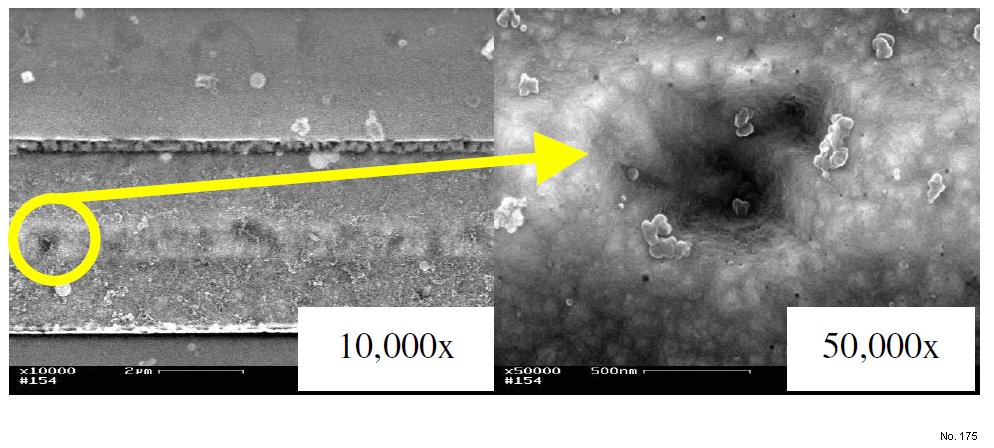
Figure 1: SEM images of the silicon substrate after plasma etching of the oxygen containing amorphous silicon spikes.