Alphabetical Index
Browse by Elements
Keyword Search
Dry Etchants
Dry and Wet Etchants
Wet Etchants
Bulk Etchants
Layer Etchants
Nano Etchants
Single Crystal Etchants
Thin Film Etchants
Thin Foil Etchants
Wafer Etchants
Al Etchants
Cd Etchants
Ga Etchants
Ge Etchants
In Etchants
New Etchants
Other Etchants
Si Etchants
Zn Etchants
Help
Home
Molten Polysilicon Filaments
Material Name: Silicon
Record No.: 176
Primary Chemical Element in Material: Si
Sample Type: Wafer
Uses: No data
Etchant Name: None
Etching Method: No data
Etchant (Electrolyte) Composition: No data
Procedure (Condition): No data
Note: For all the ESD stressed ICs, the defect is always
localized on the drain side of the GGNMOS gate
contact. A SEM image obtained after removing the
silicon oxide by plasma etching shows two holes at
the gate and silicon substrate level (Figure 1). The
presence of these holes is explained by the
preferential etching of ESD induced polysilicon
filaments. These filaments originate from the gate.
They extend into the silicon substrate thus partially short-circuiting the gate to drain p-n junction. This
“weak point” in the protection structure was also
confirmed on several protection test structures.
Reference: Félix Beaudoin, et al., Laser Beam Based ESD Defect Localization in ICs, ISTFA 2002, Proceedings of the 28th International Symposium for Testing and Failure Analysis, 3-7 November 2002, Phoenix Civic Center, Phoenix, Arizona, pp. 543-551.
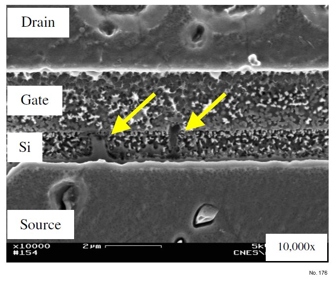
Figure 1: SEM image of the GGNMOS gate contact
after plasma etching revealing two molten
polysilicon filaments.