Alphabetical Index
Browse by Elements
Keyword Search
Dry Etchants
Dry and Wet Etchants
Wet Etchants
Bulk Etchants
Layer Etchants
Nano Etchants
Single Crystal Etchants
Thin Film Etchants
Thin Foil Etchants
Wafer Etchants
Al Etchants
Cd Etchants
Ga Etchants
Ge Etchants
In Etchants
New Etchants
Other Etchants
Si Etchants
Zn Etchants
Help
Home
Gate Conductor (GC) Short
Material Name: No data
Record No.: 177
Primary Chemical Element in Material: No data
Sample Type: Wafer
Uses: No data
Etchant Name: None
Etching Method: No data
Etchant (Electrolyte) Composition: No data
Procedure (Condition): No data
Note: Liquid crystal hotspot analysis and emission
microscopy were employed to localize the defect, but
no significant information could be gleaned from
these methods. As a result, detailed circuit layout
review coupled with layer by layer deprocessing and
cross-sections were used to isolate the fail. Cross-sections
in the suspect area showed that certain
isolated gate lines were much wider than expected,
resulting in a substantial loss of alignment margin,
and thus a high probability of contact to GC shorts,
see figure 1.
Reference: Luis Andrade, Timothy Bynum, Richard Doyle, Brian Flaherty, David Grammer, Chris Jacobs,
Mark Luzar, Eric McDaniel, Dave Ricks, Randall Stanley, Tom Taylor, Targeted Defect Analysis for Yield Improvement, ISTFA 2002, Proceedings of the 28th International Symposium for Testing and Failure Analysis, 3-7 November 2002, Phoenix Civic Center, Phoenix, Arizona, pp. 571-577.
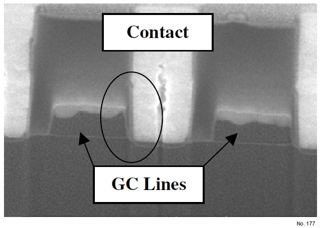
Figure 1: Cross-section image showing a contact to gate conductor (GC) short.