Alphabetical Index
Browse by Elements
Keyword Search
Dry Etchants
Dry and Wet Etchants
Wet Etchants
Bulk Etchants
Layer Etchants
Nano Etchants
Single Crystal Etchants
Thin Film Etchants
Thin Foil Etchants
Wafer Etchants
Al Etchants
Cd Etchants
Ga Etchants
Ge Etchants
In Etchants
New Etchants
Other Etchants
Si Etchants
Zn Etchants
Help
Home
Unfilled Contact
Material Name: No data
Record No.: 178
Primary Chemical Element in Material: No data
Sample Type: Wafer
Uses: No data
Etchant Name: None
Etching Method: No data
Etchant (Electrolyte) Composition: No data
Procedure (Condition): No data
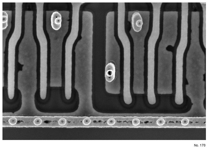
Note: Figure 1 shows a SEM photograph of the
defect found on the unit with successful FA. The
defect was an unfilled contact, with an intact liner.
This defect was not found by inline inspection
because all contacts are unfilled at the time of the
inspection, therefore at that inspection layer, the
contact would not have looked defective. Defects such as this help to explain a low OHR, however,
continued physical FA efforts are ongoing and will
be needed to improve the OHR. Because the OHR is
a direct measure of inline inspection capability and
thus the short loop yield enhancement capability, it is
perhaps the single most important result from the
logic mapping process.
Reference: Brady R. Benware, Driving Baseline Yields on ASICs using Logic Mapping, ISTFA 2002, Proceedings of the 28th International Symposium for Testing and Failure Analysis, 3-7 November 2002, Phoenix Civic Center, Phoenix, Arizona, pp. 579-586.

Figure 1: SEM picture of an un-filled contact defect obtained through PFA.