Alphabetical Index
Browse by Elements
Keyword Search
Dry Etchants
Dry and Wet Etchants
Wet Etchants
Bulk Etchants
Layer Etchants
Nano Etchants
Single Crystal Etchants
Thin Film Etchants
Thin Foil Etchants
Wafer Etchants
Al Etchants
Cd Etchants
Ga Etchants
Ge Etchants
In Etchants
New Etchants
Other Etchants
Si Etchants
Zn Etchants
Help
Home
Silicon Defect with Very Gross Electrical Leakage
Material Name: Silicon
Record No.: 179
Primary Chemical Element in Material: Si
Sample Type: Wafer
Uses: No data
Etchant Name: None
Etching Method: No data
Etchant (Electrolyte) Composition: No data
Procedure (Condition): No data
Note: No data
Reference: Erick M. Spory, N-Channel Sub-Threshold Leakage “Pipes” Generated From
Micro-Twinning Near Shallow Trench Isolation Interface, ISTFA 2002, Proceedings of the 28th International Symposium for Testing and Failure Analysis, 3-7 November 2002, Phoenix Civic Center, Phoenix, Arizona, pp. 599-606.
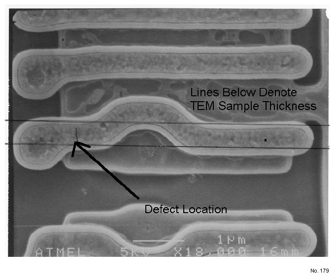
Figure 1: Top-down SEM photo of known failing location deprocessed to polysilicon and active. The
horizontal lines indicate the actual final TEM sample thickness.

Figure 2: SEM photo on specific transistor known for failing very gross electrical leakage (i.e., greater
than 5 uA). Note silicon defect decorations following a 20 second Wright etch.